ZHCSLA4E May 2020 – October 2024 TPS61378-Q1
PRODUCTION DATA
- 1
- 1 特性
- 2 应用
- 3 说明
- 4 Device Comparison Table
- 5 Pin Configuration and Functions
- 6 Specifications
-
7 Detailed Description
- 7.1 Overview
- 7.2 Functional Block Diagram
- 7.3
Feature Description
- 7.3.1 VCC Power Supply
- 7.3.2 Input Undervoltage Lockout (UVLO)
- 7.3.3 Enable and Soft Start
- 7.3.4 Shut Down
- 7.3.5 Switching Frequency Setting
- 7.3.6 Spread Spectrum Frequency Modulation
- 7.3.7 Adjustable Peak Current Limit
- 7.3.8 Bootstrap
- 7.3.9 Load Disconnect
- 7.3.10 MODE/SYNC Configuration
- 7.3.11 Overvoltage Protection (OVP)
- 7.3.12 Output Short Protection/Hiccup
- 7.3.13 Power-Good Indicator
- 7.3.14 Thermal Shutdown
- 7.4 Device Functional Modes
-
8 Application and Implementation
- 8.1 Application Information
- 8.2
Typical Application
- 8.2.1 Design Requirements
- 8.2.2 Detailed Design Procedure
- 8.2.3 Application Curves
- 9 Power Supply Recommendations
- 10Layout
- 11Device and Documentation Support
- 12Revision History
- 13Mechanical, Packaging, and Orderable Information
8.2.3 Application Curves
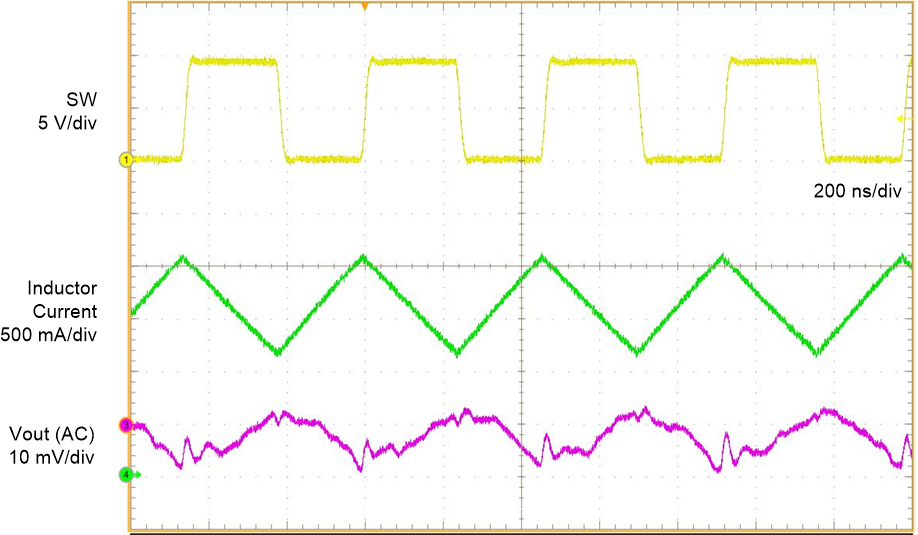 Figure 8-5 Switching Waveform VIN =
5 V,
 VOUT = 9 V, IOUT = 800 mA, FPWM
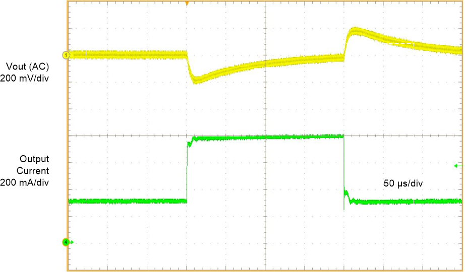 Figure 8-7 Load Transient VIN = 5 V,
VOUT = 9 V, IOUT = 300 mA to 800 mA, FPWM
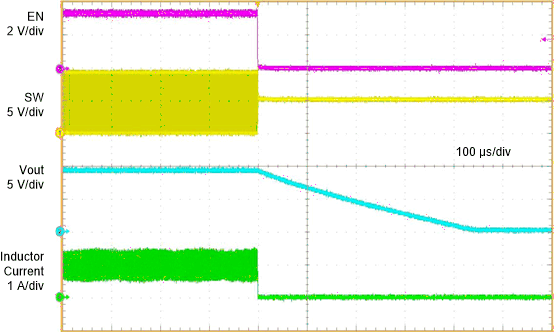 Figure 8-9 Shutdown from EN Waveforms
 VIN = 5 V, VOUT = 9 V, IOUT = 500 mA, FPWM
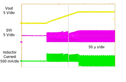 Figure 8-11 Short Circuit Recovery
VIN = 5 V,
 VOUT = 9 V, IOUT = 0 mA, FPWM
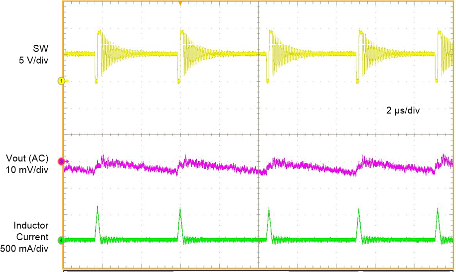 Figure 8-6 Switching Waveform VIN =
5 V,
 VOUT = 9 V, IOUT = 0 mA, Auto PFM
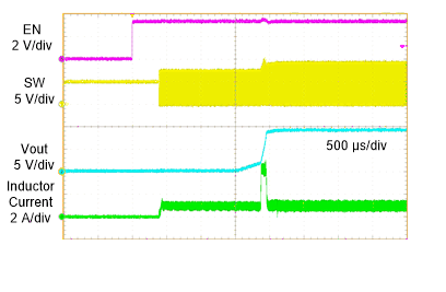 Figure 8-8 Start-up from EN Waveform
VIN = 5 V, VOUT = 9 V, IOUT = 500 mA, FPWM
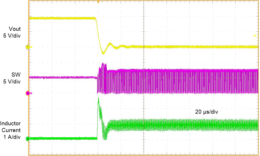 Figure 8-10 Short Circuit Protection
VIN = 5 V,
 VOUT = 9 V, FPWM
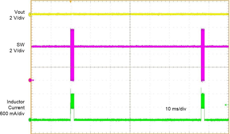 Figure 8-12 Hiccup Short Circuit Protection
 VIN = 5 V, VOUT = 9 V, FPWM