SLVS432F September 2002 – June 2015 TPS62050 , TPS62051 , TPS62052 , TPS62054 , TPS62056
PRODUCTION DATA.
- 1 Features
- 2 Applications
- 3 Description
- 4 Typical Application Schematic
- 5 Revision History
- 6 Device Comparison Table
- 7 Pin Configuration and Functions
- 8 Specifications
- 9 Detailed Description
- 10Application and Implementation
- 11Power Supply Recommendations
- 12Layout
- 13Device and Documentation Support
- 14Mechanical, Packaging, and Orderable Information
10 Application and Implementation
NOTE
Information in the following applications sections is not part of the TI component specification, and TI does not warrant its accuracy or completeness. TI’s customers are responsible for determining suitability of components for their purposes. Customers should validate and test their design implementation to confirm system functionality.
10.1 Application Information
The TPS6205x family of devices are high-efficiency synchronous step-down DC-DC converters ideally suited for systems powered from a 1-cell or 2-cell Li-Ion battery or from a 3-cell to 5-cell NiCd, NiMH, or alkaline battery.
10.2 Typical Applications
10.2.1 Standard Circuit for Adjustable Version
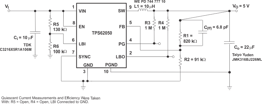 Figure 6. Standard Circuit for Adjustable Version
10.2.1.1 Design Requirements
The design guidelines provide a component selection to operate the adjustable device within the Recommended Operating Conditions.
Table 1. Bill of Materials for Adjustable Version
| REFERENCE | PART NUMBER | VALUE | MANUFACTURER |
|---|---|---|---|
| Ci | C3216X5R1A106M | 10 µF | TDK |
| Co | JMK316BJ226ML | 22 µF | Taiyo Yuden |
| L1 | WE PD 74477710 | 10 µH | Wurth |
| IC1 | TPS62050 | - | Texas Instruments |
| R1 | generic metal film resistor; tolerance 1% | 820 kΩ (depending on desired output voltage) | — |
| R2 | generic metal film resistor; tolerance 1% | 91 kΩ (depending on desired output voltage) | — |
| R3, R4 | generic metal film resistor; tolerance 1% | 1 MΩ | — |
| R5 | generic metal film resistor; tolerance 1% | 130 kΩ | — |
| R6 | generic metal film resistor; tolerance 1% | 100 kΩ | — |
| C(ff) | generic ceramic capacitor; COG | 6.8 pF | — |
10.2.1.2 Detailed Design Procedure
All graphs have been generated using the circuit as shown unless otherwise noted. For output voltages other than 5 V, the fixed-voltage versions were used. The resistors R1, R2, and the feed forward capacitor (Cff) are removed and the feedback pin is directly connected to the output.

Table 2. Values for Resistor Combinations and Feedback Capacitors
| NOMINAL OUTPUT VOLTAGE | EQUATION | POSSIBLE RESISTOR COMBINATION | TYPICAL FEEDBACK CAPACITOR |
|---|---|---|---|
| 0.7 V | R1 = 0.4 × R2 | R1 = 270 k, R2 = 680 k | C(ff) = 22 pF |
| 1.2 V | R1 = 1.4 × R2 | R1 = 510 k, R2 = 360 k (1.21 V) | C(ff) = 6.8 pF |
| 1.5 V | R1 = 2 × R2 | R1 = 300 k, R2 = 150 k (1.5 V) | C(ff) = 6.8 pF |
| 1.8 V | R1 = 2.6 × R2 | R1 = 390 k, R2 = 150 k (1.80 V) | C(ff) = 6.8 pF |
| 2.5 V | R1 = 4 × R2 | R1 = 680 k, R2 = 169 k (2.51 V) | C(ff) = 6.8 pF |
| 3.3 V | R1 = 5.6 × R2 | R1 = 560 k, R2 = 100 k (3.3 V) | C(ff) = 6.8 pF |
| 5 V | R1 = 9 × R2 | R1 = 820 k, R2 = 91 k (5 V) | C(ff) = 6.8 pF |
10.2.1.2.1 Inductor Selection
A 10-µH minimum inductor must be used with the TPS6205x family of devices. Values larger than 22 µH or smaller than 10 µH may cause stability problems due to the internal compensation of the regulator. After choosing the inductor value of typically 10 µH, two additional inductor parameters must be considered: the current rating of the inductor and the DC resistance. The DC resistance of the inductance directly influences the efficiency of the converter. Therefore, an inductor with lowest DC resistance must be selected for highest efficiency. To avoid saturation of the inductor, the inductor must be rated at least for the maximum output current plus half the inductor ripple current which is calculated using Equation 3.
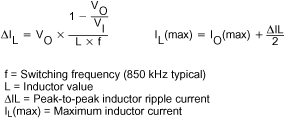
The highest inductor current occurs at maximum VIN . A more conservative approach is to select the inductor current rating just for the maximum switch current of the TPS6205x device, which is 1.4 A maximum. See Table 3 for inductors that have been tested for operation with the TPS6205x devices.
Table 3. Inductors
| MANUFACTURER | TYPE | INDUCTANCE | DC RESISTANCE | SATURATION CURRENT |
|---|---|---|---|---|
| TDK | SLF7032T-100M1R4SLF7032T-220M96SLF7045T-100M1R3SLF7045T-100MR90 | 10 µH ±20% 22 µH ±20% 10 µH ±20% 22 µH ±20% |
53 mΩ ±20% 110 mΩ ±20% 36 mΩ ±20% 61 mΩ ±20% |
1.4 A 0.96 A 1.3 A 0.9 A |
| Sumida | CDR74B | 10 µH | 70 mΩ | 1.65 A |
| CDR74B | 22 µH | 130 mΩ | 1.12 A | |
| CDH74 | 10 µH | 49 mΩ | 1.8 A | |
| CDH74 | 22 µH | 110 mΩ | 1.23 A | |
| CDR63B | 10 µH | 140 mΩ | 1 A | |
| CDRH4D28 | 10 µH | 128 mΩ | 1 A | |
| CDRH5D28 | 10 µH | 48 mΩ | 1.3 A | |
| CDRH5D18 | 10 µH | 92 mΩ | 1.2 A | |
| Coilcraft | DT3316P-153 | 15 µH | 60 mΩ | 1.8 A |
| DT3316P-223 | 22 µH | 84 mΩ | 1.5 A | |
| Wuerth | WE-PD 744 778 10 | 10 µH | 72 mΩ | 1.68 A |
| WE-PD 744 777 10 | 10 µH | 49 mΩ | 1.84 A | |
| WE-PD 744 778 122 | 22 µH | 190 mΩ | 1.07A | |
| WE-PD 744 777 122 | 22 µH | 110 mΩ | 1.23 A |
10.2.1.2.2 Output Capacitor Selection
The output capacitor must have a minimum value of 22 µF. For best performance, a low ESR ceramic output capacitor is needed.
For completeness, use Equation 4 to calculate the RMS ripple current.

The overall output ripple voltage is the sum of the voltage spike caused by the output capacitor ESR plus the voltage ripple caused by charge and discharging the output capacitor, as shown in Equation 5.

The highest output voltage ripple occurs at the highest input voltage VI.
10.2.1.2.3 Input Capacitor Selection
Because the buck converter has a pulsating input current, a low ESR input capacitor is required for best input voltage filtering and minimizing the interference with other circuits caused by high input voltage spikes. The input capacitor must have a minimum value of 10 µF and can be increased without any limit for better input voltage filtering. The input capacitor must be rated for the maximum input ripple current calculated as:

The worst-case RMS ripple current occurs at D = 0.5 and is calculated as: IRMS = IO/2. Ceramic capacitors have a good performance because of their low ESR value and they are less sensitive to voltage transients compared to tantalum capacitors. Place the input capacitor as close as possible to the input pin of the IC for best performance.
Table 4. Capacitors
| MANUFACTURER | PART NUMBER | SIZE | VOLTAGE | CAPACITANCE | TYPE |
|---|---|---|---|---|---|
| Taiyo Yuden | JMK212BJ106MG | 0805 | 6.3 V | 10 µF | Ceramic |
| JMK316BJ106ML | 1206 | 6.3 V | 10 µF | Ceramic | |
| JMK316BJ226ML | 1206 | 6.3 V | 22 µF | Ceramic | |
| LMK316BJ475ML | 1206 | 10 V | 4.7 µF(1) | Ceramic | |
| EMK316BJ475ML | 1206 | 16 V | 4.7 µF(1) | Ceramic | |
| EMK325BJ106KN-T | 1210 | 16 V | 10 µF | Ceramic | |
| Kemet | C1206C106M9PAC | 1206 | 6.3 V | 10 µF | Ceramic |
| TDK | C2012X5R0J106M | 0805 | 6.3 V | 10 µF | Ceramic |
| C3216X5R0J226M | 1206 | 6.3 V | 22 µF | Ceramic | |
| C3216X5R1A106M | 1206 | 10 V | 10 µF | Ceramic |
10.2.1.2.4 Feedforward Capacitor
The feedforward capacitor (C(ff) shown in Figure 5) improves the performance in SKIP mode. The comparator is faster; therefore, there is less voltage ripple at the output in SKIP mode. Use the values listed in Table 2. Larger values decrease stability in fixed frequency PWM mode. If the TPS6205x devices are only operated in fixed frequency PWM mode, the feedforward capacitor is not needed.
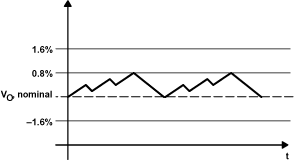 Figure 7. Power-Save Mode Output Voltage Thresholds
The converter enters the fixed frequency PWM mode again as soon as the output voltage falls below the comparator low 2 threshold set to 1.6% below VO, nominal.
10.2.1.3 Application Curves
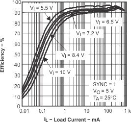 Figure 8. TPS62050 Efficiency vs Load Current
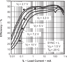 Figure 10. TPS62052 Efficiency vs Load Current
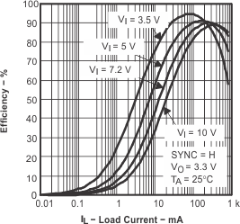 Figure 12. TPS62056 Efficiency vs Load Current
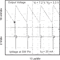 Figure 14. Output Voltage Ripple in Skip Mode
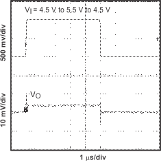 Figure 16. Line Transient Response in PWM Mode
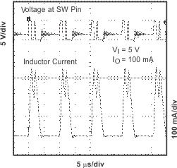 Figure 18. V(SWITCH) and IL
(Inductor Current) in Skip Mode
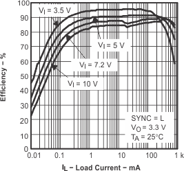 Figure 9. TPS62056 Efficiency vs Load Current
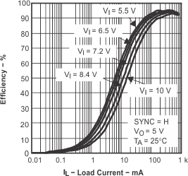 Figure 11. TPS62050 Efficiency vs Load Current
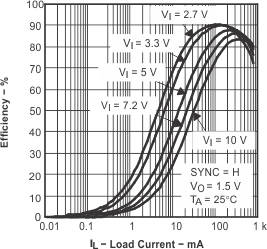 Figure 13. TPS62052 Efficiency vs Load Current
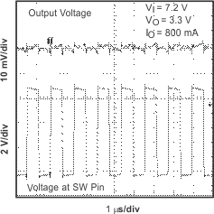 Figure 15. Output Voltage Ripple in PWM Mode
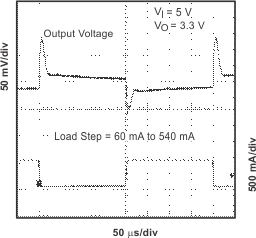 Figure 17. Load Transient Response
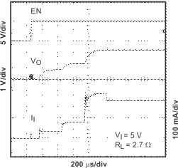 Figure 19. Start-up Timing
10.2.2 Standard Circuit for Fixed Voltage Version
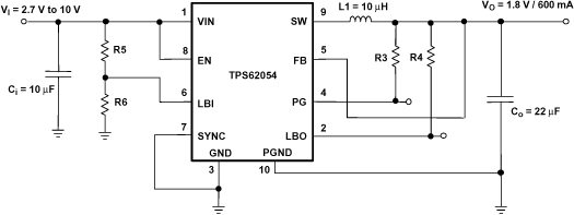 Figure 20. Standard Circuit for Fixed Voltage Version
10.2.2.1 Design Requirements
The design guidelines provide a component selection to operate the device within the Recommended Operating Conditions.
Table 5. Bill of Materials for Fixed Voltage Versions
| REFERENCE | PART NUMBER | VALUE | MANUFACTURER |
|---|---|---|---|
| Ci | C3216X5R1A106M | 10 µF | TDK |
| Co | JMK316BJ226ML | 22 µF | Taiyo Yuden |
| L1 | WE PD 74477710 | 10 µH | Wurth |
| IC1 | TPS62054 | — | Texas Instruments |
| R3, R4 | generic metal film resistor; tolerance 1% | 1 MΩ | — |
| R5 | generic metal film resistor; tolerance 1% | 130 kΩ | — |
| R6 | generic metal film resistor; tolerance 1% | 100 kΩ | — |
10.2.2.2 Detailed Design Procedure
Connect the feedback pin (FB) to the pad of the output capacitor. The pullup resistors for pins PG and LBO are typically chosen as 100 kΩ each. The input capacitor must be placed as close to the VIN pin as possible.
10.2.2.3 Application Curves
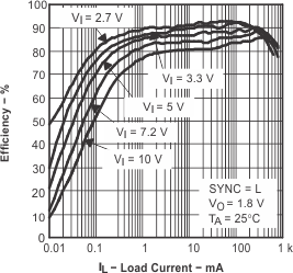 Figure 21. TPS62054 Efficiency vs Load Current in PFM Mode
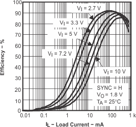 Figure 22. TPS62054 Efficiency vs Load Current in PWM Mode
10.3 System Examples
The TPS62050 device is used to generate an output voltage of 0.7 V. With such low output voltages, the inductor discharges very slowly. This leads to a high-output voltage ripple in power-save mode (SYNC = GND). Therefore, TI recommends using a larger output capacitor to keep the output ripple low. With an output capacitor of 47 µF, the output voltage ripple is less than 40 mVPP.
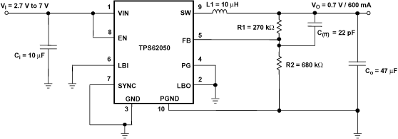 Figure 23. Converter for 0.7-V Output Voltage