SLVS432F September 2002 – June 2015 TPS62050 , TPS62051 , TPS62052 , TPS62054 , TPS62056
PRODUCTION DATA.
- 1 Features
- 2 Applications
- 3 Description
- 4 Typical Application Schematic
- 5 Revision History
- 6 Device Comparison Table
- 7 Pin Configuration and Functions
- 8 Specifications
- 9 Detailed Description
- 10Application and Implementation
- 11Power Supply Recommendations
- 12Layout
- 13Device and Documentation Support
- 14Mechanical, Packaging, and Orderable Information
12 Layout
12.1 Layout Guidelines
All capacitors must be soldered as close as possible to the IC.
For information on the PCB layout, see the user's guide, SLVU081.
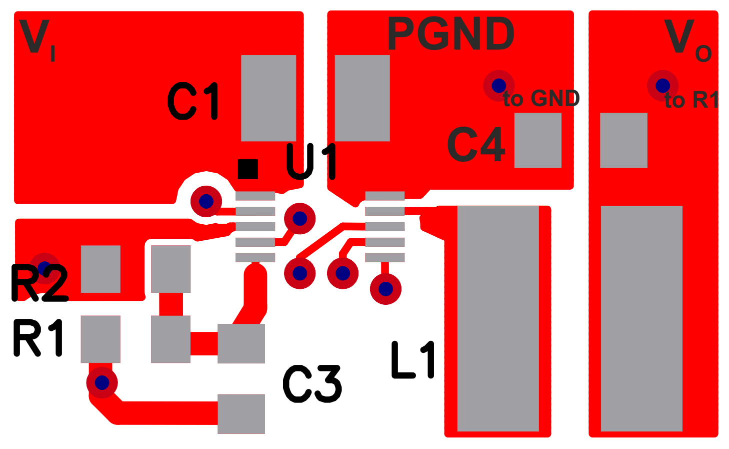
Keep the feedback track as short as possible. Any coupling to the FB pin may cause additional output voltage ripple. The feedback connection from the output capacitor C4 to R1 of the feedback network is made directly from the pad of C4 as shown by the via. The connection of GND with PGND is done similarly directly at the PGND pad of C4. Uncritical signals like the connections for LBI, LBO, and PG are not shown for better readability.
12.2 Layout Example
 Figure 24. Layout
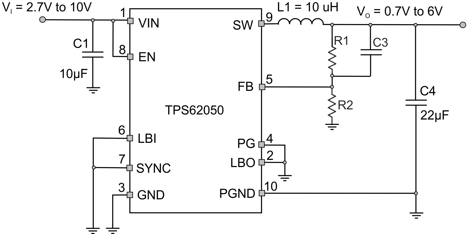
 Figure 25. Associated Layout Schematic