SLVSA95B March 2010 – July 2015 TPS62060 , TPS62061 , TPS62063
PRODUCTION DATA.
- 1 Features
- 2 Applications
- 3 Description
- 4 Revision History
- 5 Device Comparison Table
- 6 Pin Configuration and Functions
- 7 Specifications
- 8 Detailed Description
- 9 Application and Implementation
- 10Power Supply Recommendations
- 11Layout
- 12Device and Documentation Support
- 13Mechanical, Packaging, and Orderable Information
7 Specifications
7.1 Absolute Maximum Ratings
over operating free-air temperature range (unless otherwise noted)(1)| MIN | MAX | UNIT | |||
|---|---|---|---|---|---|
| Voltage(2) | AVIN, PVIN | –0.3 | 7 | V | |
| EN, MODE, FB | –0.3 | VIN +0.3 < 7 | |||
| SW | –0.3 | 7 | |||
| Current (source) | Peak output | Internally limited | A | ||
| Temperature | Junction, TJ | –40 | 125 | °C | |
| Storage, Tstg | –65 | 150 | |||
(1) Stresses beyond those listed under Absolute Maximum Ratings may cause permanent damage to the device. These are stress ratings only, which do not imply functional operation of the device at these or any other conditions beyond those indicated under Recommended Operating Conditions. Exposure to absolute-maximum-rated conditions for extended periods may affect device reliability.
(2) All voltage values are with respect to network ground terminal.
7.2 ESD Ratings
| VALUE | UNIT | |||
|---|---|---|---|---|
| V(ESD) | Electrostatic discharge | Human body model (HBM), per ANSI/ESDA/JEDEC JS-001(1) | ±2000 | V |
| Charged-device model (CDM), per JEDEC specification JESD22-C101(2) | ±1000 | |||
(1) JEDEC document JEP155 states that 500-V HBM allows safe manufacturing with a standard ESD control process.
(2) JEDEC document JEP157 states that 250-V CDM allows safe manufacturing with a standard ESD control process.
7.3 Recommended Operating Conditions
| MIN | NOM | MAX | UNIT | ||
|---|---|---|---|---|---|
| AVIN , PVIN | Supply voltage | 2.7 | 6 | V | |
| Output current capability | 1600 | mA | |||
| Output voltage for adjustable voltage | 0.8 | VIN | V | ||
| L | Effective inductance | 0.7 | 1 | 1.6 | µH |
| COUT | Effective output capacitance | 4.5 | 10 | 22 | µF |
| TA | Operating ambient temperature(1) | –40 | 85 | °C | |
| TJ | Operating junction temperature | –40 | 125 | °C | |
(1) In applications where high power dissipation and/or poor package thermal resistance is present, the maximum ambient temperature may have to be derated. Maximum ambient temperature (TA(max)) is dependent on the maximum operating junction temperature (TJ(max)), the maximum power dissipation of the device in the application (PD(max)), and the junction-to-ambient thermal resistance of the part/package in the application (θJA), as given by the following equation: TA(max)= TJ(max)–(θJA × PD(max))
7.4 Thermal Information
| THERMAL METRIC(1) | TPS62060, TPS62061, TPS62063 | UNIT | |
|---|---|---|---|
| DSG (WSON) | |||
| 8 PINS | |||
| RθJA | Junction-to-ambient thermal resistance | 64.68 | °C/W |
| RθJC(top) | Junction-to-case (top) thermal resistance | 80.6 | °C/W |
| RθJB | Junction-to-board thermal resistance | 34.63 | °C/W |
| ψJT | Junction-to-top characterization parameter | 1.65 | °C/W |
| ψJB | Junction-to-board characterization parameter | 35.02 | °C/W |
| RθJC(bot) | Junction-to-case (bottom) thermal resistance | 6.61 | °C/W |
(1) For more information about traditional and new thermal metrics, see the Semiconductor and IC Package Thermal Metrics application report, SPRA953.
7.5 Electrical Characteristics
Over full operating ambient temperature range, typical values are at TA = 25°C. Unless otherwise noted, specifications apply for condition VIN = EN = 3.6 V. External components CIN = 10 μF 0603, COUT = 10 μF 0603, L = 1 μH, see the parameter measurement information.| PARAMETER | TEST CONDITIONS | MIN | TYP | MAX | UNIT | |
|---|---|---|---|---|---|---|
| SUPPLY | ||||||
| VIN | Input voltage range | 2.7 | 6 | V | ||
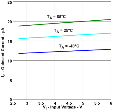
| IQ | Operating quiescent current | IOUT = 0 mA, device operating in PFM mode and device not switching |
18 | 25 | μA | |
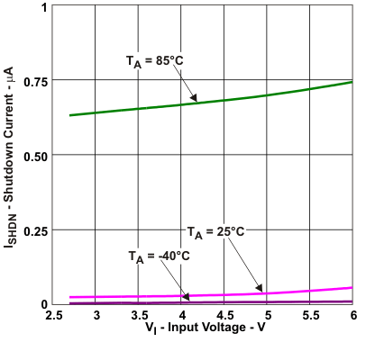
| ISD | Shutdown current | EN = GND, current into AVIN and PVIN | 0.1 | 1 | μA | |
| VUVLO | Undervoltage lockout threshold | Falling | 1.73 | 1.78 | 1.83 | V |
| Rising | 1.9 | 1.95 | 1.99 | |||
| ENABLE, MODE | ||||||
| VIH | High level input voltage | 2.7 V ≤ VIN ≤ 6 V | 1 | 6 | V | |
| VIL | Low level input voltage | 2.7 V ≤ VIN ≤ 6 V | 0 | 0.4 | V | |
| IIN | Input bias current | Pin tied to GND or VIN | 0.01 | 1 | μA | |
| POWER SWITCH | ||||||
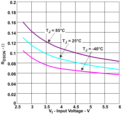
| RDS(on) | High-side MOSFET on-resistance | VIN = 3.6 V (2) | 120 | 180 | mΩ | |
| VIN = 5 V(2) | 95 | 150 | ||||
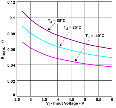
| Low-side MOSFET on-resistance | VIN = 3.6 V(2) | 90 | 130 | mΩ | ||
| VIN = 5 V(2) | 75 | 100 | ||||
| ILIMF | Forward current limit MOSFET high-side and low-side | 2.7V ≤ VIN ≤ 6 V | 1800 | 2250 | 2700 | mA |
| TSD | Thermal shutdown | Increasing junction temperature | 150 | °C | ||
| Thermal shutdown hysteresis | Decreasing junction temperature | 10 | °C | |||
| OSCILLATOR | ||||||
| fSW | Oscillator frequency | 2.7 V ≤ VIN ≤ 6 V | 2.6 | 3 | 3.4 | MHz |
| OUTPUT | ||||||
| Vref | Reference voltage | 600 | mV | |||
| VFB(PWM) | Feedback voltage PWM mode | PWM operation, MODE = VIN , 2.7 V ≤ VIN ≤ 6 V, 0 mA load |
–1.5% | 0% | 1.5% | |
| VFB(PFM) | Feedback voltage PFM mode, voltage positioning | device in PFM mode, voltage positioning active(1) | 1% | |||
| VFB | Load regulation | –0.5 | %/A | |||
| Line regulation | 0 | %/V | ||||
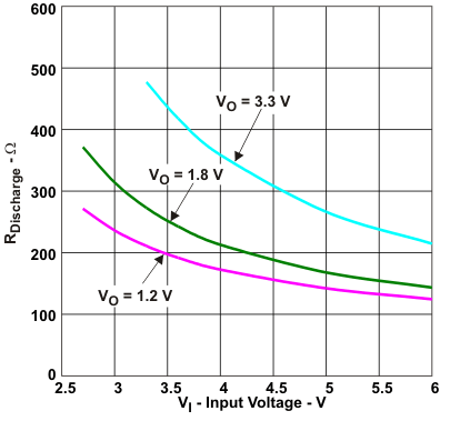
| R(Discharge) | Internal discharge resistor | Activated with EN = GND, 2 V ≤ VIN≤ 6 V, 0.8 ≤ VOUT ≤ 3.6 V | 75 | 200 | 1450 | Ω |
| tSTART | Start-up time | Time from active EN to reach 95% of VOUT | 500 | μs | ||
(1) In PFM mode, the internal reference voltage is set to typ. 1.01 × Vref. See the parameter measurement information.
(2) Maximum value applies for TJ = 85°C
7.6 Dissipation Ratings(1)(2)
| PACKAGE | RθJA | POWER RATING TA = ≤ 25°C |
DERATING FACTOR ABOVE TA = 25°C |
|
|---|---|---|---|---|
| DSG | 75°C/W | 1300 mW | 13 mW/°C | |
(1) Maximum power dissipation is a function of TJ(max), θJA and TA. The maximum allowable power dissipation at any allowable ambient temperature is PD = (TJ(max) – TA)/ θJA.
(2) This thermal data measured with high-K board (4 layers according to JESD51-7 JEDEC Standard).
7.7 Typical Characteristics
