ZHCSMB6E March 2010 – October 2020 TPS62065 , TPS62067
PRODUCTION DATA
- 1 特性
- 2 应用
- 3 说明
- 4 Revision History
- 5 Device Comparison Table
- 6 Pin Configuration and Functions
- 7 Specifications
- 8 Detailed Description
- 9 Application and Implementation
- 10Power Supply Recommendations
- 11Layout
- 12Device and Documentation Support
- 13Mechanical, Packaging, and Orderable Information
8.3.2 Power Good Output (TPS62067)
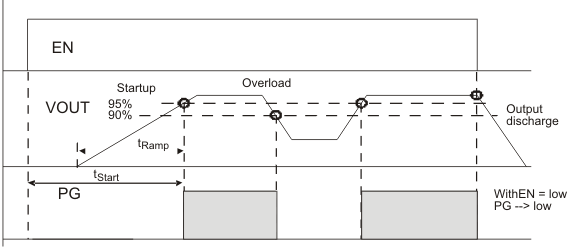
This function is available in the TPS62067. The power good output is an open-drain output and requires an external pullup resistor. The circuit is active once the device is enabled and AVIN is above the undervoltage lockout threshold VUVLO. It is driven by an internal comparator connected to the FB voltage. The PG output provides a high level once the feedback voltage exceeds typically 95% of its nominal value. The PG output is driven to low level once the feedback voltage falls below typically 90% of its nominal value. The PG output is activated with an internal delay of 5 µs.
The PG open-drain output transistor is turned on immediately with EN = Low level and pulls the output low. The external pullup resistor can be connected to any voltage rail lower or equal the voltage applied to AVIN of the device. The value of the pullup resistor must be carefully selected to limit the current into the PG pin to maximum 1 mA. The external pullup resistor can be connected to VOUT or another voltage rail which does not exceed the VIN level. The current flowing through the pullup resistor impacts the current consumption of the application circuit in shutdown mode.
The shutdown current of the device does not include the current through the external pullup and internal open-drain stage. The PG signal can be used for sequencing various converters or to reset a microcontroller.
 Figure 8-1 Power Good Output Pg