ZHCSMB6E March   2010  – October 2020 TPS62065 , TPS62067

PRODUCTION DATA  

  1. 特性
  2. 应用
  3. 说明
  4. Revision History
  5. Device Comparison Table
  6. Pin Configuration and Functions
  7. Specifications
    1. 7.1 Absolute Maximum Ratings
    2. 7.2 ESD Ratings
    3. 7.3 Recommended Operating Conditions
    4. 7.4 Thermal Information
    5. 7.5 Electrical Characteristics
    6. 7.6 Typical Characteristics
  8. Detailed Description
    1. 8.1 Overview
    2. 8.2 Functional Block Diagram
    3. 8.3 Feature Description
      1. 8.3.1 Mode Selection (TPS62065)
      2. 8.3.2 Power Good Output (TPS62067)
      3. 8.3.3 Enable
      4. 8.3.4 Clock Dithering
      5. 8.3.5 Undervoltage Lockout
      6. 8.3.6 Thermal Shutdown
    4. 8.4 Device Functional Modes
      1. 8.4.1 Soft Start
      2. 8.4.2 Power Save Mode
      3. 8.4.3 Dynamic Voltage Positioning
      4. 8.4.4 100% Duty Cycle Low Dropout Operation
      5. 8.4.5 Internal Current Limit and Fold-Back Current Limit for Short Circuit Protection
      6. 8.4.6 Output Capacitor Discharge
  9. Application and Implementation
    1. 9.1 Application Information
    2. 9.2 Typical Application
      1. 9.2.1 Design Requirements
      2. 9.2.2 Detailed Design Procedure
        1. 9.2.2.1 Output Voltage Setting
        2. 9.2.2.2 Output Filter Design (Inductor and Output Capacitor)
          1. 9.2.2.2.1 Inductor Selection
          2. 9.2.2.2.2 Output Capacitor Selection
          3. 9.2.2.2.3 Input Capacitor Selection
        3. 9.2.2.3 Checking Loop Stability
      3. 9.2.3 Application Curves
    3. 9.3 System Example
      1. 9.3.1 TPS62067 Adjustable 1.8-V Output
  10. 10Power Supply Recommendations
  11. 11Layout
    1. 11.1 Layout Guidelines
    2. 11.2 Layout Example
  12. 12Device and Documentation Support
    1. 12.1 Device Support
      1. 12.1.1 Third-Party Products Disclaimer
    2. 12.2 Related Links
    3. 12.3 Receiving Notification of Documentation Updates
    4. 12.4 Support Resources
    5. 12.5 Trademarks
    6. 12.6 Electrostatic Discharge Caution
    7. 12.7 Glossary
  13. 13Mechanical, Packaging, and Orderable Information

封装选项

机械数据 (封装 | 引脚)
散热焊盘机械数据 (封装 | 引脚)
订购信息

Typical Characteristics

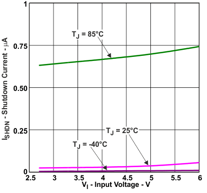
GUID-E129BB5B-B38A-4A7A-847E-7D5ABAB588DA-low.gifFigure 7-1 Shutdown Current vs Input Voltage and Ambient Temperature
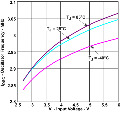
GUID-A8AF580E-7797-470D-B814-BD0D946A2AEA-low.gifFigure 7-3 Oscillator Frequency vs Input Voltage
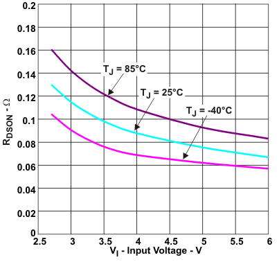
GUID-5FE3AB89-017B-4664-A3AC-16BA64FD4990-low.gifFigure 7-5 RDSON High-Side Switch
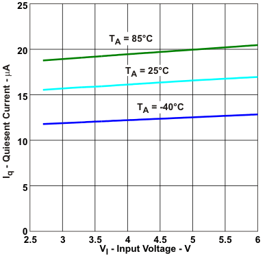
GUID-17CA5BB6-444B-41C9-8DB7-119BF101037F-low.gifFigure 7-2 Quiescent Current vs Input Voltage
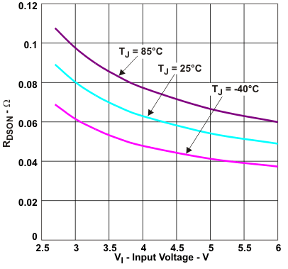
GUID-08B05726-8238-4235-ADC4-474AB68B5129-low.gifFigure 7-4 RDSON Low-Side Switch
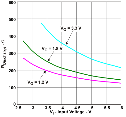
GUID-57CC4ED4-5F4D-4DE7-9725-321EC316AFD3-low.gifFigure 7-6 Rdischarge vs Input Voltage