ZHCSD80B january 2015 – august 2023 TPS62065-Q1 , TPS62067-Q1
PRODUCTION DATA
- 1
- 1 特性
- 2 应用
- 3 说明
- 4 Revision History
- 5 Device Comparison Table
- 6 Pin Configuration and Functions
- 7 Specifications
- 8 Parameter Measurement Information
-
9 Detailed Description
- 9.1 Overview
- 9.2 Functional Block Diagram
- 9.3
Feature Description
- 9.3.1 Mode Selection (TPS62065-Q1) and Forced PWM Mode (TPS62067A-Q1)
- 9.3.2 Power Good (PG, TPS62067x-Q1)
- 9.3.3 Enable
- 9.3.4 Shutdown and Output Discharge
- 9.3.5 Soft Start
- 9.3.6 Undervoltage Lockout (UVLO)
- 9.3.7 Internal Current Limit and Foldback Current Limit For Short-Circuit Protection
- 9.3.8 Clock Dithering
- 9.3.9 Thermal Shutdown
- 9.4 Device Functional Modes
- 10Application and Implementation
- 11Device and Documentation Support
- 12Mechanical, Packaging, and Orderable Information
Abstract
Table 7-1 Table of Graphs
| FIGURE | |||
|---|---|---|---|
| Shutdown Current | Input Voltage and Ambient Temperature | Figure 7-1 | |
| Quiescent Current | Input Voltage | Figure 7-2 | |
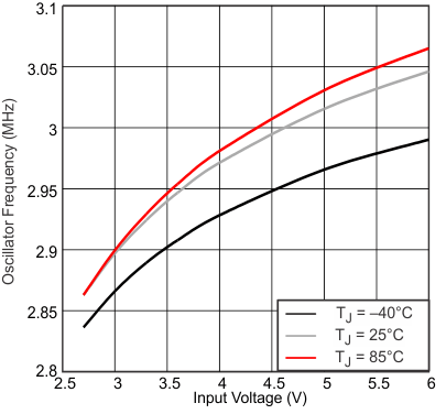
| Oscillator Frequency | Input Voltage | Figure 7-3 | |
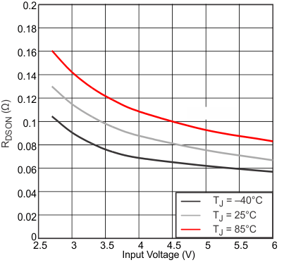
| Static Drain-Source On-State Resistance | Input Voltage, Low-Side Switch | Figure 7-4 | |
| Input Voltage, High-Side Switch | Figure 7-5 | ||
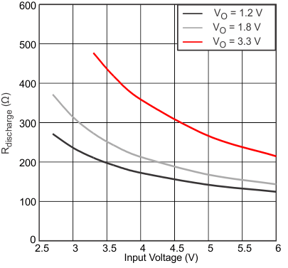
| RDISCHARGE | Input Voltage vs. VOUT | Figure 7-6 | |
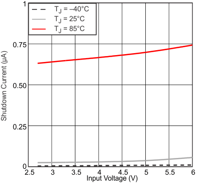 Figure 7-1 Shutdown Current vs Input Voltage and Ambient Temperature
| High-Side Switch |
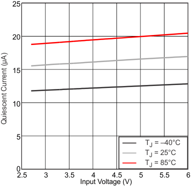 Figure 7-2 Quiescent Current vs Input Voltage
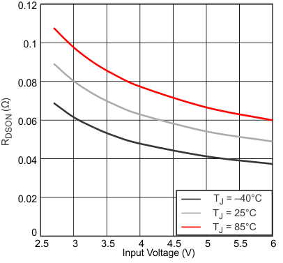
| Low-Side Switch |
