ZHCS442F September 2011 – November 2016 TPS62080 , TPS62080A , TPS62081 , TPS62082
PRODUCTION DATA.
- 1 特性
- 2 应用范围
- 3 说明
- 4 修订历史记录
- 5 Device Comparison Table
- 6 Pin Configuration and Functions
- 7 Specifications
- 8 Detailed Description
- 9 Application and Implementation
- 10Power Supply Recommendations
- 11Layout
- 12器件和文档支持
- 13机械、封装和可订购信息
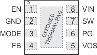
6 Pin Configuration and Functions
space
DSG Package
8-Pin WSON With Thermal Pad
(Top View)

space
space
Pin Functions
| PIN | I/O | DESCRIPTION | |
|---|---|---|---|
| NAME | NO. | ||
| EN | 1 | IN | Device Enable Logic Input. Logic HIGH enables the device, logic LOW disables the device and turns it into shutdown. Do not leave floating. |
| GND | 2 | PWR | Power and Signal Ground. |
| MODE | 3 | IN | Snooze Mode Enable Logic Input. Logic HIGH enables the Snooze Mode, logic LOW disables the Snooze Mode. Do not leave floating. |
| FB | 4 | IN | Feedback Pin for the internal control loop. Connect this pin to the external feedback divider for the adjustable output versions. For the fixed output voltage versions, this pin must be left floating or connected to GND. |
| VOS | 5 | IN | Output Voltage Sense Pin for the internal control loop. Must be connected to output voltage. |
| PG | 6 | OUT | Power Good open drain output. This pin is pulled to low if the output voltage is below regulation limits. Can be left floating if not used. |
| SW | 7 | PWR | Switch Pin connected to the internal MOSFET switches and inductor terminal. Connect the inductor of the output filter here. |
| VIN | 8 | PWR | Power Supply Voltage Input. |
| Exposed Thermal Pad | — | — | Connect it to GND. The thermal pad must be soldered to achieve appropriate power dissipation and mechanical reliability. |