ZHCS442F September 2011 – November 2016 TPS62080 , TPS62080A , TPS62081 , TPS62082
PRODUCTION DATA.
- 1 特性
- 2 应用范围
- 3 说明
- 4 修订历史记录
- 5 Device Comparison Table
- 6 Pin Configuration and Functions
- 7 Specifications
- 8 Detailed Description
- 9 Application and Implementation
- 10Power Supply Recommendations
- 11Layout
- 12器件和文档支持
- 13机械、封装和可订购信息
9 Application and Implementation
NOTE
Information in the following applications sections is not part of the TI component specification, and TI does not warrant its accuracy or completeness. TI’s customers are responsible for determining suitability of components for their purposes. Customers should validate and test their design implementation to confirm system functionality.
9.1 Application Information
The TPS62080 and TPS62080A are synchronous step-down converter whose output voltage is adjusted by component selection. The following section discusses the design of the external components to complete the power supply design for several input and output voltage options by using typical applications as a reference. The TPS62081 and TPS62082 provide a fixed output volage which do not need an external resistor divider.
9.2 Typical Application
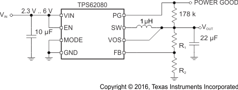 Figure 7. Typical Application Schematic
9.2.1 Design Requirements
For this design example, use Table 2 as the input parameters.
Table 2. Design Parameters
| DESIGN PARAMETER | EXAMPLE VALUE |
|---|---|
| Input voltage | 2.3 V to 6 V |
| Output voltage | 1.2 V |
| Output ripple voltage | < 20 mV |
| Maximum output current | 1.2 A |
9.2.2 Detailed Design Procedure
Table 3 lists the components used for the example.
Table 3. List of Components
| REFERENCE | DESCRIPTION | MANUFACTURER |
|---|---|---|
| C1 | 10 uF, Ceramic Capacitor, 6.3 V, X5R, size 0603 | Std |
| C2 | 22 uF, Ceramic Capacitor, 6.3 V, X5R, size 0805, GRM21BR60J226ME39L | Murata |
| L1 | 1.0 µH, Power Inductor, 2.2 A, size 3 × 3 × 1.2 mm, XFL3012-102MEB | Coilcraft |
| R1 | Depending on the output voltage of TPS62080, 1%; Not populated for TPS62081, TPS62082; | Std |
| R2 | 39.2k, Chip Resistor, 1/16W, 1%, size 0603 | Std |
| R3 | 178k, Chip Resistor, 1/16W, 1%, size 0603 | Std |
9.2.2.1 Setting the Output Voltage
The TPS608x devices are available as fixed and adjustable output voltage versions. The fixed voltage versions are internally programmed to a fixed output voltage, whereas the adjustable output voltage version needs to be programmed via an external voltage divider to set the desired output voltage.
9.2.2.1.1 Adjustable Output Voltage Version
For the adjustable output voltage version, an external resistor divider is used. By selecting R1 and R2, the output voltage is programmed to the desired value.
When the output voltage is regulated, the typical voltage at the FB pin is VFB for the adjustable devices. The following equation can be used to calculate R1 and R2.

For best accuracy, R2 should be kept smaller than 40kΩ to ensure that the current flowing through R2 is at least 100 times larger than IFB. Changing towards a lower value increases the robustness against noise injection. Changing towards higher values reduces the input current. For lowest input current during Snooze Mode, it is recommended to use a fixed output voltage version such as TPS62081 and TPS62082.
9.2.2.2 Output Filter Design
The inductor and the output capacitor together provide a low pass filter. To simplify this process, Table 4 outlines possible inductor and capacitor value combinations for most applications. Checked cells represent combinations that are proven for stability by simulation and lab test. Further combinations should be checked for each individual application.
Table 4. Matrix of Output Capacitor and Inductor Combinations
| L [µH](3) | COUT [µF](3) | ||||
|---|---|---|---|---|---|
| 10 | 22 | 47 | 100 | 150 | |
| 0.47 | |||||
| 1 | + | +(1)(2) | + | + | |
| 2.2 | + | + | + | + | |
| 4.7 | |||||
9.2.2.3 Inductor Selection
The main parameters for the inductor selection are the inductor value and then the saturation current of the inductor. To calculate the maximum inductor current under static load conditions, Equation 3 is given.
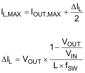
where
- IOUT,MAX = Maximum output current
- ΔIL = Inductor current ripple
- fSW = Switching frequency
- L = Inductor value
TI recommends to choose the saturation current for the inductor 20%~30% higher than the IL,MAX, out of Equation 3. A higher inductor value is also useful to lower ripple current, but increases the transient response time as well. The following inductors are recommended for use.
Table 5. List of Recommended Inductors
| INDUCTANCE [µH] |
CURRENT RATING [mA] |
DIMENSIONS L x W x H [mm3] |
DC RESISTANCE [mΩ typ] |
TYPE | MANUFACTURER |
|---|---|---|---|---|---|
| 1.0 | 2500 | 3 x 3 x 1.2 | 35 | XFL3012-102ME | Coilcraft |
| 1.0 | 1650 | 3 x 3 x 1.2 | 40 | LQH3NPN1R0NJ0 | Murata |
| 2.2 | 2500 | 4 x 3.7 x 1.65 | 49 | LQH44PN2R2MP0 | Murata |
| 2.2 | 1600 | 3 x 3 x 1.2 | 81 | XFL3012-222ME | Coilcraft |
9.2.2.4 Capacitor Selection
The input capacitor is the low impedance energy source for the converter which helps to provide stable operation. A low ESR multilayer ceramic capacitor is recommended for best filtering and should be placed between VIN and GND as close as possible to those pins. For most applications 10 μF is sufficient, though a larger value reduces input current ripple.
The architecture of the TPS6208X allows the use of tiny ceramic output capacitors with low equivalent series resistance (ESR). These capacitors provide low output voltage ripple and are recommended. To keep its resistance up to high frequencies and to get narrow capacitance variation with temperature, it's recommended to use X7R or X5R dielectric. The TPS6208x is designed to operate with an output capacitance of 10 µF to 100 µF and beyond, as outlined in Table 4. Load transient testing and measuring the bode plot are good ways to verify stability with larger capacitor values.
Table 6. List of Recommended Capacitors
| CAPACITANCE [µF] |
TYPE | DIMENSIONS L x W x H [mm3] |
MANUFACTURER |
|---|---|---|---|
| 10 | GRM188R60J106M | 0603: 1.6 x 0.8 x 0.8 | Murata |
| 22 | GRM188R60G226M | 0603: 1.6 x 0.8 x 0.8 | Murata |
| 22 | GRM21BR60J226M | 0805: 2.0 x 1.2 x 1.25 | Murata |
9.2.3 Application Curves
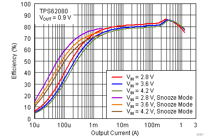 Figure 8. Efficiency vs Load Current
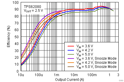 Figure 10. Efficiency vs Load Current
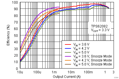 Figure 12. Efficiency vs Load Current
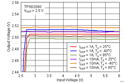 Figure 14. Output Voltage vs Input Voltage
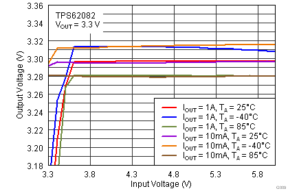 Figure 16. Output Voltage vs Input Voltage
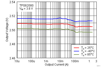 Figure 18. Output Voltage vs Load Current
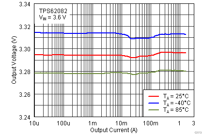 Figure 20. Output Voltage vs Load Current
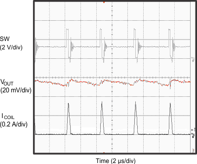
| VIN = 3.3 V, VOUT = 1.2 V, Load Current = 10 mA |
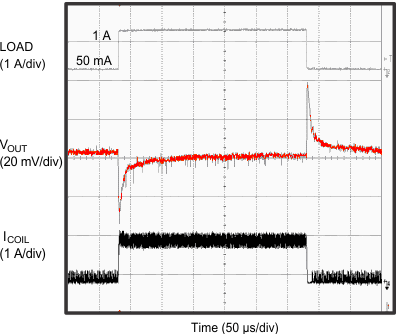
| VIN = 3.3 V, VOUT = 1.2 V, Load Current = 50 mA to 1 A |
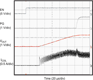
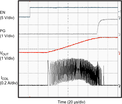
| VIN = 3.3 V, VOUT = 1.2 V, Load = 2.2 Ω |
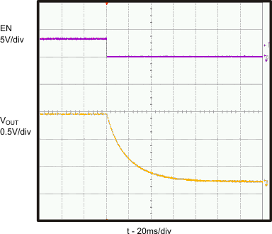
| VIN = 3.3 V, VOUT = 1.2 V, No Load |
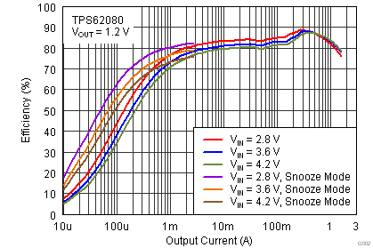 Figure 9. Efficiency vs Load Current
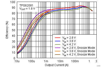 Figure 11. Efficiency vs Load Current
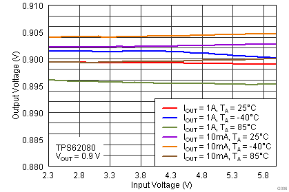 Figure 13. Output Voltage vs Input Voltage
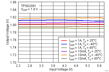 Figure 15. Output Voltage vs Input Voltage
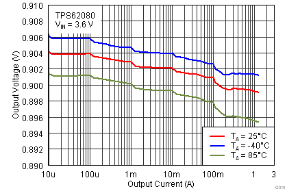 Figure 17. Output Voltage vs Load Current
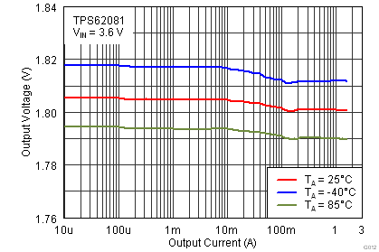 Figure 19. Output Voltage vs Load Current
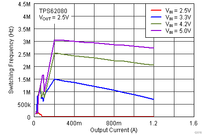
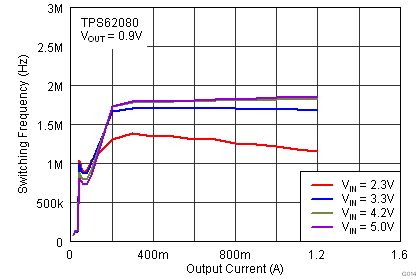 Figure 21. Switching Frequency vs Load Current
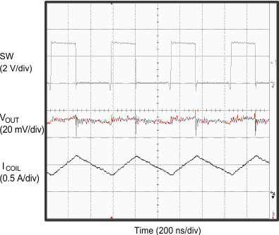
| VIN = 3.3 V, VOUT = 1.2 V, Load Current = 500 mA |
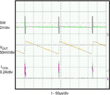
| VIN = 3.3 V, VOUT = 1.2 V, Load Current = 2 mA |
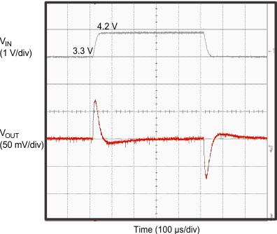
| VIN = 3.3 V to 4.2 V, VOUT = 1.2 V, Load = 2.2 Ω |
| VIN = 3.3 V, VOUT = 1.2 V, No Load |