ZHCSBE5C August 2013 – November 2021 TPS62090-Q1
PRODUCTION DATA
- 1 特性
- 2 应用
- 3 说明
- 4 Revision History
- 5 Pin Configuration and Functions
- 6 Specifications
-
7 Detailed Description
- 7.1 Overview
- 7.2 Functional Block Diagram
- 7.3
Feature Description
- 7.3.1 Enable and Disable (EN)
- 7.3.2 Soft Start (SS) and Hiccup Current Limit During Start-Up
- 7.3.3 Voltage Tracking (SS)
- 7.3.4 Short-Circuit Protection (Hiccup Mode)
- 7.3.5 Output Discharge Function
- 7.3.6 Power Good Output (PG)
- 7.3.7 Frequency Set Pin (FREQ)
- 7.3.8 Undervoltage Lockout (UVLO)
- 7.3.9 Thermal Shutdown
- 7.3.10 Charge Pump (CP, CN)
- 7.4 Device Functional Modes
- 8 Application and Implementation
- 9 Power Supply Recommendations
- 10Layout
- 11Device and Documentation Support
- 12Mechanical, Packaging, and Orderable Information
8.3 System Examples
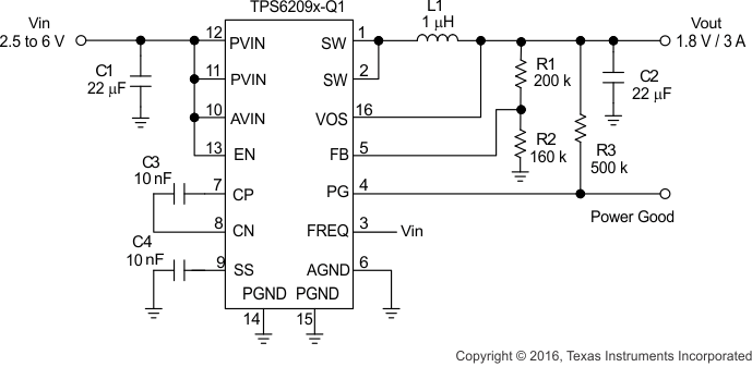
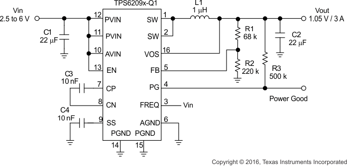
Figure 8-22, Figure 8-23, and Figure 8-24 show additional circuits for varying voltage options.
 Figure 8-22 1.5-V Adjustable Version Operating at 2.8 MHz
 Figure 8-23 1.8-V Adjustable Version Operating at 1.4 MHz
 Figure 8-24 1.05-V Adjustable Version Operating at 1.4 MHz