ZHCSH71A September 2017 – December 2017 TPS62097-Q1
PRODUCTION DATA.
7 Detailed Description
7.1 Overview
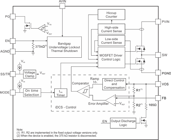
The TPS62097-Q1 synchronous step-down converter is based on the iDCS-Control (Industrial Direct Control with Seamless transition into Power Save Mode) topology. The control topology not only keeps the advantages of DCS-Control, but also provides other features:
- Forced PWM mode over the whole load range
- Selectable PWM switching frequency
- 1% output voltage accuracy
- Output voltage sequencing and tracking
The iDCS-Control topology operates in PWM (Pulse Width Modulation) mode for medium to heavy load conditions and in Power Save Mode (PSM) at light load conditions. Or the forced PWM mode removes power save mode operation and operates the device always at its nominal switching frequency.
In PWM mode, the device operates with a predictive On-time switching pulse. A constant switching frequency over the input and output voltage range is achieved by using an input and output voltage feed forward to set the on-time, as shown in Table 1. In PSM mode, the switching frequency is reduced to achieve high efficiency over the entire load current range. Since iDCS-Control supports both operation modes within a single building block, the transition from PWM mode to Power Save Mode is seamless and without effects on the output voltage.
7.2 Functional Block Diagram

7.3 Feature Description
7.3.1 100% Duty Cycle Mode
The device offers a low input to output voltage dropout by entering 100% duty cycle mode, when the input voltage reaches the level of the output voltage. In this mode the high-side MOSFET switch is constantly turned on and the low-side MOSFET is switched off. The minimum input voltage to maintain output regulation, depending on the load current and output voltage, is calculated as:
where
- VIN(min) = Minimum input voltage to maintain a minimum output voltage
- IOUT = Output current
- RDS(on) = High side FET on-resistance
- RL = Inductor ohmic resistance (DCR)
When the device operates close to 100% duty cycle mode, the TPS62097-Q1 can't enter Power Save Mode regardless of the load current if the input voltage decreases to typically 15% above the output voltage. The device maintains output regulation in PWM mode.
7.3.2 Switch Current Limit and Hiccup Short Circuit Protection
The switch current limit prevents the devices from high inductor current and from drawing excessive current from the battery or input voltage rail. Excessive current might occur with a shorted/saturated inductor or a heavy load/shorted output circuit condition. If the inductor current reaches the threshold ILIMF, the high-side MOSFET is turned off and the low-side MOSFET is turned on to ramp down the inductor current. Once this switch current limit is triggered 32 times, the devices stop switching and enable the output discharge. The devices then automatically start a new startup after a typical delay time of 100µs has passed. This is HICCUP short circuit protection and is implemented to reduce the current drawn during a short circuit condition. The devices repeat this mode until the high load condition disappears.
When the device is in forced PWM mode, the negative current limit of the low-side MOSFET is active. The negative current limit prevents excessive current from flowing back through the inductor to the input.
7.3.3 Under Voltage Lockout (UVLO)
To avoid mis-operation of the device at low input voltages, an under voltage lockout is implemented, which shuts down the devices at voltages lower than VUVLO with a hysteresis of 100mV.
7.3.4 Thermal Shutdown
The device goes into thermal shutdown and stops switching once the junction temperature exceeds TJSD. Once the device temperature falls below the threshold by 20°C, the device returns to normal operation automatically.
7.4 Device Function Modes
7.4.1 Enable and Disable (EN)
The device is enabled by setting the EN pin to a logic High. Accordingly, shutdown mode is forced if the EN pin is pulled Low with a shutdown current of typically 0.7 μA.
In shutdown mode, the internal power switches as well as the entire control circuitry are turned off. An internal resistor of 165 Ω discharges the output via the VOS pin smoothly. The output discharge function also works when thermal shutdown, undervoltage lockout or HICCUP short circuit protection are triggered.
An internal pull-down resistor of 375 kΩ is connected to the EN pin when the EN pin is Low. The pull-down resistor is disconnected when the EN pin is High.
7.4.2 Power Save Mode and Forced PWM Mode (MODE)
The MODE pin is a multi-functional pin that allows the device operation in forced PWM mode or PWM/PSM mode, and to select the PWM switching frequency.
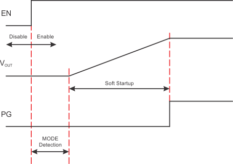
Once the EN pin is pulled high, the IC enables internal circuit blocks and prepares to ramp the output up. The period between the rising edge of the EN pin and the beginning of the power stage switching is called the MODE detection time, typically 50µs. During the MODE detection time period, shown in Figure 3, the PWM switching frequency and operating mode are set by the MODE pin status, as shown in Table 1.
The PWM switching frequency can't be changed after the detection time period. Only when the device is set in PWM/PSM mode during the MODE detection time period (MODE = AGND), it is possible to switch between PWM/PSM and forced PWM operation modes by toggling the MODE pin with a GPIO pin of a micro-controller, for example. The other four MODE pin selections force the device in PWM mode only.
 Figure 3. Power Up Sequence
Table 1. Switching Frequency and Mode Selection
| Typical PWM Switching Frequency (MHz) | Resistance at MODE pin (E24 EIA Value) |
Toggle MODE pin after MODE detection | ON-Time Equation | Operating Mode |
|---|---|---|---|---|
| 1.50 | 8.2kΩ ±5% | No | tON = 667ns x VOUT / VIN | Forced PWM |
| 1.75 | 18kΩ ±5% | No | tON = 571ns x VOUT / VIN | Forced PWM |
| 2.00 | AGND | Yes | tON = 500ns x VOUT / VIN | PWM/PSM and Forced PWM |
| 2.25 | 39kΩ ±5% | No | tON = 444ns x VOUT / VIN | Forced PWM |
| 2.50 | 75kΩ ±5% or Open | No | tON = 400ns x VOUT / VIN | Forced PWM |
Connecting the MODE pin to AGND with a resistor or leaving the MODE pin open forces the device into PWM mode for the whole load range. The device operates with a constant switching frequency that allows simple filtering of the switching frequency for noise sensitive applications. In forced PWM mode, the efficiency is lower than that of PSM at light load.
Connecting the MODE pin to the AGND pin enables Power Save Mode with an automatic transition between PWM and Power Save Mode. As the load current decreases and the inductor current becomes discontinuous, the device enters Power Save Mode operation automatically. In Power Save Mode, the switching frequency is reduced and estimated by Equation 2. In Power Save Mode, the output voltage rises slightly above the nominal output voltage, as shown in Figure 13. This effect is minimized by increasing the output capacitor.

When the device operates close to 100% duty cycle mode, the TPS62097-Q1 can't enter Power Save Mode regardless of the load current if the input voltage decreases to typically 15% above the output voltage. The device maintains output regulation in PWM mode.
7.4.3 Soft Startup (SS/TR)
The TPS62097-Q1 programs its output voltage ramp rate with the SS/TR pin. Connecting an external capacitor to SS/TR enables output soft startup to reduce inrush current from the input supply. The device charges the capacitor voltage to the input supply voltage with a constant current of typically 7.5μA. The FB pin voltage follows the SS/TR pin voltage until the internal reference voltage of 0.8V is reached. The soft startup time is calculated using Equation 3. Keep the SS/TR pin floating to set the minimum startup time.

An active pull-down circuit is connected to the SS/TR pin. It discharges the external soft startup capacitor in case of disable, UVLO, thermal shutdown and HICCUP short circuit protection.
7.4.4 Voltage Tracking (SS/TR)
The SS/TR pin is externally driven by another voltage source to achieve output voltage tracking. The application circuit is shown in Figure 4. From 0 V to 0.8 V, the internal reference voltage to the internal error amplifier follows the SS/TR pin voltage. When the SS/TR pin voltage is above 0.8 V, the voltage tracking is disabled and the FB pin voltage is regulated at 0.8 V. The device achieves ratiometric or coincidental (simultaneous) output tracking, as shown in Figure 5.
The R2 value should be set properly to achieve accurate voltage tracking by taking 7.5 µA soft startup current into account. 1 kΩ or smaller is a sufficient value for R2.
For decreasing SS/TR pin voltage, the device doesn't sink current from the output when the device is in PSM. So the resulting decreases of the output voltage may be slower than the SS/TR pin voltage if the load is light. When driving the SS/TR pin with an external voltage, do not exceed the voltage rating of the SS/TR pin which is VIN+0.3V.
7.4.5 Power Good (PG)
The TPS62097-Q1 has a power good output. The PG pin goes high impedance once the output voltage is above 95% of the nominal voltage, and is driven low once the output voltage falls below typically 90% of the nominal voltage. The PG pin is an open drain output and is specified to sink up to 1mA. The power good output requires a pull-up resistor connected to any voltage rail less than 6V. The PG signal can be used for sequencing of multiple rails by connecting it to the EN pin of other converters. Leave the PG pin floating when not used. Table 2 shows the PG pin logic.
Table 2. PG Pin Logic
| Device Conditions | Logic Status | ||
|---|---|---|---|
| High Z | Low | ||
| Enable | EN = High, VFB ≥ VPG | √ | |
| EN = Low, VFB ≤ VPG | √ | ||
| Shutdown | EN = Low | √ | |
| Thermal Shutdown | TJ > TJSD | √ | |
| UVLO | 0.7 V < VIN < VUVLO | √ | |
| Power Supply Removal | VIN ≤ 0.7 V | √ | |