SLVS585E July 2005 – June 2015 TPS62110 , TPS62111 , TPS62112 , TPS62113
PRODUCTION DATA.
- 1 Features
- 2 Applications
- 3 Description
- 4 Typical Application Schematic
- 5 Revision History
- 6 Device Comparison Table
- 7 Pin Configuration and Functions
- 8 Specifications
- 9 Detailed Description
- 10Application and Implementation
- 11Power Supply Recommendations
- 12Layout
- 13Device and Documentation Support
- 14Mechanical, Packaging, and Orderable Information
12 Layout
12.1 Layout Guidelines
A proper layout is critical for the operation of a switched-mode power supply (SMPS), even more at high switching frequencies. Therefore, the PCB layout of the TPS6211x devices demands careful attention to ensure operation and to get the performance specified. A poor layout can lead to issues like poor regulation (both line and load), stability and accuracy weaknesses, increased EMI radiation, and noise sensitivity.
Provide low inductive and resistive paths for loops with high di/dt. Therefore, paths conducting the switched load current should be as short and wide as possible. The input and output capacitance should be placed as close as possible to the IC pins and parallel wiring over long distances as well as narrow traces should be avoided. Provide low capacitive paths (with respect to all other nodes) for wires with high dv/dt. Therefore, keep the SW node small. Loops which conduct an alternating current should outline an area as small as possible, as this area is proportional to the energy radiated.
Sensitive nodes like FB and LBI need to be connected with short wires and not nearby high dv/dt signals (that is, SW). The FB resistors, R1 and R2, and LBI resistors, R5 and R6, should be kept close to the IC and connect directly to those pins and AGND. The 1-µF capacitor on VINA should connect directly from VINA to AGND.
All grounds (GND, AGND, and PGND) are directly connected to the exposed thermal pad. The exposed thermal pad must be soldered to the circuit board for mechanical reliability and to achieve appropriate power dissipation.
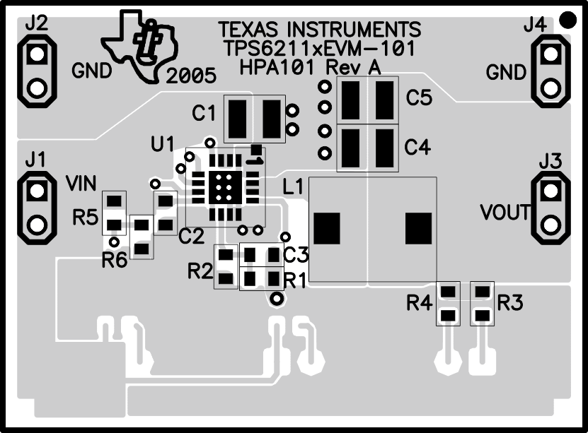
See Figure 22 for the recommended layout of the TPS6211x.
12.2 Layout Example
 Figure 22. Recommended Layout