SLVS585E July   2005  – June 2015 TPS62110 , TPS62111 , TPS62112 , TPS62113

PRODUCTION DATA.  

  1. Features
  2. Applications
  3. Description
  4. Typical Application Schematic
  5. Revision History
  6. Device Comparison Table
  7. Pin Configuration and Functions
  8. Specifications
    1. 8.1 Absolute Maximum Ratings
    2. 8.2 ESD Ratings
    3. 8.3 Recommended Operating Conditions
    4. 8.4 Thermal Information
    5. 8.5 Electrical Characteristics
    6. 8.6 Typical Characteristics
  9. Detailed Description
    1. 9.1 Overview
    2. 9.2 Functional Block Diagram
    3. 9.3 Feature Description
      1. 9.3.1 Enable
      2. 9.3.2 Low-Battery Detector (Standard Version)
      3. 9.3.3 Enable/Low-Battery Detector - Enhanced Version (TPS62113 Only)
      4. 9.3.4 Power Good Comparator
      5. 9.3.5 Undervoltage Lockout
      6. 9.3.6 Synchronization
      7. 9.3.7 Thermal Shutdown
    4. 9.4 Device Functional Modes
      1. 9.4.1 Soft Start
      2. 9.4.2 Constant-Frequency Mode of Operation (Sync = High)
      3. 9.4.3 Power Save Mode of Operation (Sync = Low)
      4. 9.4.4 100% Duty-Cycle, Low-Dropout Operation
      5. 9.4.5 No-Load Operation
  10. 10Application and Implementation
    1. 10.1 Application Information
    2. 10.2 Typical Applications
      1. 10.2.1 Standard Connection for Adjustable Version
        1. 10.2.1.1 Design Requirements
        2. 10.2.1.2 Detailed Design Procedure
          1. 10.2.1.2.1 External Component Selection
          2. 10.2.1.2.2 Inductor Selection
          3. 10.2.1.2.3 Output Capacitor Selection
          4. 10.2.1.2.4 Input Capacitor Selection
          5. 10.2.1.2.5 Feedforward Capacitor Selection
          6. 10.2.1.2.6 Recommended Capacitors
        3. 10.2.1.3 Application Curves
      2. 10.2.2 Standard Connection for Fixed-Voltage Version
        1. 10.2.2.1 Design Requirements
        2. 10.2.2.2 Detailed Design Procedure
        3. 10.2.2.3 Application Curves
    3. 10.3 System Examples
  11. 11Power Supply Recommendations
  12. 12Layout
    1. 12.1 Layout Guidelines
    2. 12.2 Layout Example
  13. 13Device and Documentation Support
    1. 13.1 Device Support
      1. 13.1.1 Third-Party Products Disclaimer
    2. 13.2 Related Links
    3. 13.3 Community Resources
    4. 13.4 Trademarks
    5. 13.5 Electrostatic Discharge Caution
    6. 13.6 Glossary
  14. 14Mechanical, Packaging, and Orderable Information

封装选项

机械数据 (封装 | 引脚)
散热焊盘机械数据 (封装 | 引脚)
订购信息

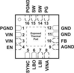
7 Pin Configuration and Functions

RSA Package
16-Pin VQFN
Top View
TPS62110 TPS62111 TPS62112 TPS62113 po_lvs585.gif

Pin Functions

PIN I/O DESCRIPTION
NAME NO.
AGND 9 I Analog ground, connect to GND and PGND.
EN 4 I Enable. A logic high enables the converter; logic low forces the device into shutdown mode reducing the supply current to less than 2 µA. Do not leave floating.
FB 10 I Feedback pin for the fixed output voltage versions. Connect to VOUT for these devices. For the adjustable versions, an external resistive divider is connected to this pin. The internal voltage divider is disabled for the adjustable versions.
GND 11, 12 I Ground
LBI 7 I Low-battery input. Do not leave floating.
LBO 6 O Open-drain, low-battery output. This pin is pulled low if LBI is below its threshold. If not used, the pin may be left floating or connected to GND.
PG 13 O Power good comparator output. This is an open-drain output. A pullup resistor should be connected between PG and VOUT. The output goes high when the output voltage is greater than 98.4% of the nominal value. If not used, the pin may be left floating or connected to GND.
PGND 1, 16 I Power ground. Connect all power grounds to this pin.
SW 14, 15 O Connect the inductor to this pin. This pin is the switch pin and connected to the drain of the internal power MOSFETS.
SYNC 5 I Input for synchronization to external clock signal. Synchronizes the converter switching frequency to an external clock signal with CMOS level. Also controls power save mode by being tied high or low.
  SYNC = HIGH: Low-noise mode enabled, fixed-frequency PWM operation is forced
  SYNC = LOW (GND): Power save mode enabled, PFM/PWM mode enabled
VIN 2, 3 I Supply voltage input (power stage)
VINA 8 I Supply voltage input (support circuits)
Exposed Thermal Pad Connect to AGND. Must be soldered to achieve appropriate power dissipation and mechanical reliability.