SLVS585E July 2005 – June 2015 TPS62110 , TPS62111 , TPS62112 , TPS62113
PRODUCTION DATA.
- 1 Features
- 2 Applications
- 3 Description
- 4 Typical Application Schematic
- 5 Revision History
- 6 Device Comparison Table
- 7 Pin Configuration and Functions
- 8 Specifications
- 9 Detailed Description
- 10Application and Implementation
- 11Power Supply Recommendations
- 12Layout
- 13Device and Documentation Support
- 14Mechanical, Packaging, and Orderable Information
8 Specifications
8.1 Absolute Maximum Ratings
over operating free-air temperature range (unless otherwise noted) (1)| MIN | MAX | UNIT | ||
|---|---|---|---|---|
| VCC | Supply voltage at VIN, VINA | –0.3 | 20 | V |
| VI | Voltage at SW | –1 | 20 | V |
| Voltage at EN, SYNC, LBO, PG | –0.3 | 20 | ||
| Voltage at LBI, FB | –0.3 | 7 | ||
| IO | Output current at SW | 2400 | mA | |
| TJ | Maximum junction temperature | 150 | °C | |
| TA | Operating free-air temperature | –40 | 85 | °C |
| Tstg | Storage temperature | –65 | 150 | °C |
(1) Stresses beyond those listed under Absolute Maximum Ratings may cause permanent damage to the device. These are stress ratings only and functional operation of the device at these or any other conditions beyond those indicated under Recommended Operating Conditions is not implied. Exposure to absolute-maximum-rated conditions for extended periods may affect device reliability.
8.2 ESD Ratings
| VALUE | UNIT | |||
|---|---|---|---|---|
| V(ESD) | Electrostatic discharge | Human body model (HBM), per ANSI/ESDA/JEDEC JS-001(1) | ±2000 | V |
| Charged-device model (CDM), per JEDEC specification JESD22-C101(2) | ±500 | |||
(1) JEDEC document JEP155 states that 500-V HBM allows safe manufacturing with a standard ESD control process.
(2) JEDEC document JEP157 states that 250-V CDM allows safe manufacturing with a standard ESD control process.
8.3 Recommended Operating Conditions
| MIN | NOM | MAX | UNIT | ||
|---|---|---|---|---|---|
| VCC | Supply voltage at VIN, VINA | 3.1 | 17 | V | |
| Maximum voltage at PG, LBO, EN, SYNC | 17 | V | |||
| TJ | Operating junction temperature | –40 | 125 | °C | |
8.4 Thermal Information
| THERMAL METRIC(1) | TPS6211x | UNIT | |
|---|---|---|---|
| RSA (VQFN) | |||
| 16 PINS | |||
| RθJA | Junction-to-ambient thermal resistance | 48.2 | °C/W |
| RθJC(top) | Junction-to-case (top) thermal resistance | 45.4 | °C/W |
| RθJB | Junction-to-board thermal resistance | 16.3 | °C/W |
| ψJT | Junction-to-top characterization parameter | 0.5 | °C/W |
| ψJB | Junction-to-board characterization parameter | 16.4 | °C/W |
| RθJC(bot) | Junction-to-case (bottom) thermal resistance | 3.3 | °C/W |
(1) For more information about traditional and new thermal metrics, see the Semiconductor and IC Package Thermal Metrics application report, SPRA953.
8.5 Electrical Characteristics
VI = 12 V, VO = 3.3 V, IO = 600 mA, EN = VI, TA = –40°C to 85°C (unless otherwise noted)| PARAMETER | TEST CONDITIONS | MIN | TYP | MAX | UNIT | ||
|---|---|---|---|---|---|---|---|
| SUPPLY CURRENT | |||||||
| VI | Input voltage | 3.1 | 17 | V | |||
| I(Q) | Operating quiescent current | IO = 0 mA, SYNC = GND, VI = 7.2 V, TA = 25°C (1) |
20 | µA | |||
| IO = 0 mA, SYNC = GND, VI = 17 V (1) | 23 | 26 | |||||
| IQ(LBI) | Quiescent current with enhanced LBI comparator version (TPS62113 only). | EN = VI , LBI = GND | 10 | µA | |||
| I(SD) | Shutdown current | EN = GND | 1.5 | 5 | µA | ||
| EN = GND, TA = 25°C, VI = 7.2 V | 1.5 | 3 | |||||
| ENABLE | |||||||
| VIH | EN high-level input voltage | 1.3 | V | ||||
| VIL | EN low-level input voltage | 0.3 | V | ||||
| EN trip-point hysteresis | 170 | mV | |||||
| Ilkg | EN input leakage current | EN = GND or VI, VI = 12 V | 0.01 | 0.2 | µA | ||
| I(EN) | EN input current | 0.6 V ≤ V(EN) ≤ 4 V | 10 | 20 | µA | ||
| V(UVLO) | Undervoltage lockout threshold | Input voltage falling | 2.8 | 3 | 3.1 | V | |
| Undervoltage lockout hysteresis | 250 | 300 | mV | ||||
| POWER SWITCH | |||||||
| RDS(ON) | P-channel MOSFET ON-resistance | VI ≥ 5.4 V; IO = 350 mA | 165 | 250 | mΩ | ||
| VI = 3.5 V; IO = 200 mA | 340 | ||||||
| VI = 3 V; IO = 100 mA | 490 | ||||||
| Ilkg | P-channel MOSFET leakage current | VDS = 17 V | 0.1 | 1 | µA | ||
| ILIMF | P-channel MOSFET current limit | VI = 7.2 V, VO = 3.3 V | 2100 | 2400 | 2600 | mA | |
| RDS(ON) | N-channel MOSFET ON-resistance | VI ≥ 5.4 V; IO = 350 mA | 145 | 200 | mΩ | ||
| VI = 3.5 V; IO = 200 mA | 170 | ||||||
| VI = 3 V; IO = 100 mA | 200 | ||||||
| Ilkg | N-channel MOSFET leakage current | VDS = 17 V | 0.1 | 2 | µA | ||
| PG OUTPUT, LBI, LBO | |||||||
| V(PG) | Power good trip voltage | VO – 1.6% | V | ||||
| Power good delay time | VO ramping positive | 50 | µs | ||||
| VO ramping negative | 200 | ||||||
| VOL | PG, LBO output-low voltage | V(FB) = 0.8 × VO nominal, IOL = 1 mA | 0.3 | V | |||
| IOL | PG, LBO sink current | 1 | mA | ||||
| Ilkg | PG, LBO output leakage current | V(FB) = VO nominal, V(LBI) = VI | 0.01 | 0.25 | µA | ||
| Minimum supply voltage for valid power good, LBI, LBO signal | 3 | V | |||||
| VLBI | LBI input trip voltage | Input voltage falling | 1.256 | V | |||
| Ilkg | LBI input leakage current | 10 | 100 | nA | |||
| LBI input trip-point accuracy |
1.5% | ||||||
| VLBI,HYS | Low-battery input hysteresis | 25 | mV | ||||
| OSCILLATOR | |||||||
| fS | Oscillator frequency | 900 | 1000 | 1100 | kHz | ||
| f(SYNC) | Synchronization range | CMOS-logic clock signal on SYNC pin | 800 | 1400 | kHz | ||
| VIH | SYNC high-level input voltage | 1.5 | V | ||||
| VIL | SYNC low-level input voltage | 0.3 | V | ||||
| Ilkg | SYNC input leakage current | SYNC = GND or VIN | 0.01 | 0.2 | µA | ||
| SYNC trip-point hysteresis | 170 | mV | |||||
| Ilkg | SYNC input leakage current | 0.6 V ≤ V(SYNC) ≤ 4 V | 10 | 20 | µA | ||
| Duty cycle of external clock signal | 30% | 90% | |||||
| OUTPUT | |||||||
| VO | Adjustable output voltage range | TPS62110 TPS62113 |
1.153 | 16 | V | ||
| VFB | Feedback voltage | TPS62110 TPS62113 |
1.153 | V | |||
| Ilkg | FB input leakage current | TPS62110 TPS62113 |
10 | 100 | nA | ||
| Feedback voltage tolerance | TPS62110 TPS62113 |
VI = 3.1 V to 17 V; 0 mA < IO < 1500 mA(3) |
–2% | 2% | |||
| Fixed output voltage tolerance(2) | TPS62111 | VI = 3.8 V to 17 V; 0 mA < IO < 1500 mA(3) |
–3% | 3% | |||
| TPS62112 | VI = 5.5 V to 17 V; 0 mA < IO < 1500 mA(3) |
–3% | 3% | ||||
| IO | Maximum output current | VI ≥ 3 V (once undervoltage lockout voltage exceeded) | 100 | mA | |||
| VI ≥ 3.5 V | 500 | ||||||
| VI ≥ 4.3 V | 1200 | ||||||
| VI ≥ 6 V | 1500 | ||||||
| Current into internal voltage divider for fixed voltage versions | 5 | µA | |||||
| η | Efficiency | VI = 7.2 V; VO = 3.3 V; IO = 600 mA | 92% | ||||
| VI = 12 V, Vo = 5 V, Io = 600 mA | |||||||
| Duty-cycle range for main switches | at 1 MHz | 10% | 100% | ||||
| Minimum ton time for main switch | 100 | ns | |||||
| TSD | Shutdown temperature | 145 | °C | ||||
| Start-up time | IO = 800 mA, VI = 12 V, Vo = 3.3 V | 1 | ms | ||||
(1) Device is not switching.
(2) The output voltage accuracy includes line and load regulation over the full temperature range TA = –40°C to 85°C. See No-Load Operation.
(3) The maximum output current depends on the input voltage. See the maximum output current for further restrictions on the minimum input voltage.
8.6 Typical Characteristics
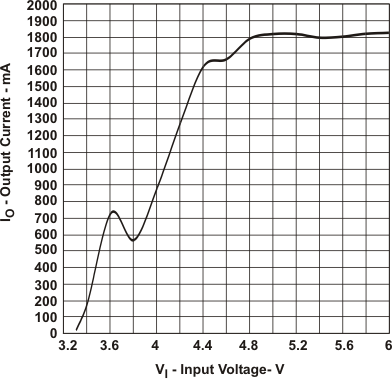
 Figure 1. TPS62111 Maximum Output Current vs Input Voltage
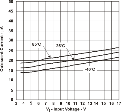
 Figure 3. Quiescent Current vs Input Voltage
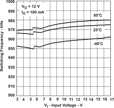
 Figure 2. Switching Frequency vs Input Voltage