SLVSAD5A July 2010 – August 2015 TPS62120 , TPS62122
PRODUCTION DATA.
- 1 Features
- 2 Applications
- 3 Description
- 4 Revision History
- 5 Device Comparison Table
- 6 Pin Configuration and Functions
- 7 Specifications
- 8 Detailed Description
- 9 Application and Implementation
- 10Power Supply Recommendations
- 11Layout
- 12Device and Documentation Support
- 13Mechanical, Packaging, and Orderable Information
6 Pin Configuration and Functions
DRV Package
6-Pin SON
Top View

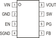
DCN Package
8-Pin SOT-23
Top View

Pin Functions
| PIN | I/O | DESCRIPTION | ||
|---|---|---|---|---|
| NAME | DFN | SOT-23 | ||
| EN | 4 | 3 | I | Pulling this pin to high activates the device. Low level shuts it down. This pin must be terminated. |
| FB | 3 | 5 | I | This is the feedback pin for the regulator. Connect external resistor-divider to this pin. |
| GND | 6 | 2 | PWR | GND supply pin. |
| PG | — | 6 | O | This pin is available in TPS62120 only. Open-drain power good output. Connect this terminal through a pullup resistor to a voltage rail up to 5.5 V or leave it open. This pin can sink 500 µA. |
| SGND | — | 4 | I | This pin is available in TPS62120 only. Open-drain output which is turned on during shutdown mode (EN = 0) or VIN is below the UVLO threshold. The output connects the SGND pin to GND through an internal MOSFET with typical 370-Ω RDS(ON). When the device is enabled (EN = 1), this output is high impedance. To discharge the output capacitor during shutdown mode, connect this pin to VOUT (output capacitor) or leave it open. |
| SW | 1 | 7 | O | This is the switch pin and is connected to the internal MOSFET switches. Connect the inductor to this terminal. Do not tie this pin to VIN, VOUT or GND. |
| VIN | 5 | 1 | PWR | VIN power supply pin. |
| VOUT | 2 | 8 | I | This pin must be connected to the output capacitor. |
| — | Exposed Thermal Pad | — | — | Exposed thermal pad available only in DRV package option. This pad must be connected to GND. |