ZHCS862E March 2012 – May 2017 TPS62125
PRODUCTION DATA.
- 1 特性
- 2 应用
- 3 说明
- 4 修订历史记录
- 5 Pin Configuration and Functions
- 6 Specifications
- 7 Detailed Description
- 8 Application and Implementation
- 9 Power Supply Recommendations
- 10Layout
- 11器件和文档支持
- 12机械、封装和可订购信息
10 Layout
10.1 Layout Guidelines
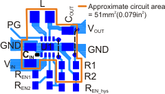
As for all switching power supplies, the layout is an important step in the design. Proper function of the device demands careful attention to PCB layout. Take care in the board layout to get the specified performance. If the layout is not carefully done, the regulator could show frequency variations, poor line and/or load regulation, stability issues as well as EMI problems. It is critical to provide a low-inductance, low-impedance ground path. Therefore, use wide and short traces for the paths conducting AC current of the DC/DC converter. The area of the AC current loop (input capacitor – TPS62125 – inductor – output capacitor) should be routed as small as possible to avoid magnetic field radiation. Therefore the input capacitor should be placed as close as possible to the IC pins as well as the inductor and output capacitor. Use a common power GND node and a different node for the signal GND to minimize the effects of ground noise. Keep the common path to the GND pin, which returns both the small signal components and the high current of the output capacitors as short as possible to avoid ground noise. A well proven practice is to merge small signal GND and power GND path at the exposed thermal pad. The FB divider network and the FB line should be routed away from the inductor and the SW node to avoid noise coupling. The VOS line should be connected as short as possible to the output, ideally to the VOUT terminal of the inductor. Keep the area of the loop VOS node – inductor – SW node small. The exposed thermal pad must be soldered to the circuit board for mechanical reliability and to achieve appropriate power dissipation.
10.2 Layout Example
 Figure 61. EVM Board Layout