ZHCSB84F November 2011 – November 2021 TPS62130 , TPS62130A , TPS62131 , TPS62132 , TPS62133
PRODUCTION DATA
- 1 特性
- 2 应用
- 3 说明
- 4 Revision History
- 5 Device Comparison Table
- 6 Pin Configuration and Functions
- 7 Specifications
- 8 Detailed Description
- 9 Application and Implementation
- 10Power Supply Recommendations
- 11Layout
- 12Device and Documentation Support
- 13Mechanical, Packaging, and Orderable Information
6 Pin Configuration and Functions
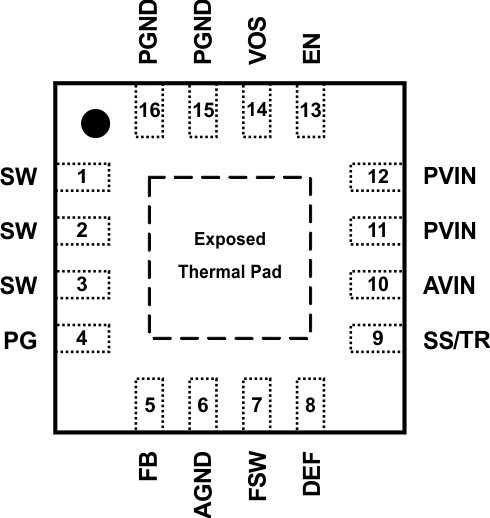
 Figure 6-1 16-Pin VQFN With Exposed Thermal Pad (RGT)Top View
Table 6-1 Pin Functions
| PIN(1) | I/O | DESCRIPTION | |
|---|---|---|---|
| NO. | NAME | ||
| 1,2,3 | SW | O | Switch node, which is connected to the internal MOSFET switches. Connect an inductor between SW and the output capacitor. |
| 4 | PG | O | Output power good (High = VOUT ready, Low = VOUT below nominal regulation); open drain (requires pullup resistor) |
| 5 | FB | I | Voltage feedback of adjustable version. Connect a resistive voltage divider to this pin. It is recommended to connect FB to AGND on fixed output voltage versions for improved thermal performance. |
| 6 | AGND | Analog Ground. Must be connected directly to the Exposed Thermal Pad and common ground plane. | |
| 7 | FSW | I | Switching Frequency Select (Low ≈ 2.5 MHz, High ≈ 1.25 MHz(2) for typical operation)(3) |
| 8 | DEF | I | Output voltage scaling (Low = nominal, High = nominal + 5%)(3) |
| 9 | SS/TR | I | Soft-Start/Tracking Pin. An external capacitor connected to this pin sets the internal voltage reference rise time. It can be used for tracking and sequencing. |
| 10 | AVIN | I | Supply voltage for control circuitry. Connect to the same source as PVIN. |
| 11,12 | PVIN | I | Supply voltage for power stage. Connect to the same source as AVIN. |
| 13 | EN | I | Enable input (High = enabled, Low = disabled)(3) |
| 14 | VOS | I | Output voltage sense pin and connection for the control loop circuitry |
| 15,16 | PGND | Power Ground. Must be connected directly to the Exposed Thermal Pad and common ground plane. | |
| Exposed Thermal Pad | Must be connected to AGND (pin 6), PGND (pin 15,16), and common ground plane. See the Layout Example. Must be soldered to achieve appropriate power dissipation and mechanical reliability. | ||
(1) For more information about connecting pins, see the Detailed Description and Application and Implementation sections.
(2) Connect FSW to VOUT or PG in this case.
(3) An internal pulldown resistor keeps logic level low if pin is
floating.