SLVSDV2 March 2017 TPS62136
PRODUCTION DATA.
- 1 Features
- 2 Applications
- 3 Description
- 4 Revision History
- 5 Device Comparison Table
- 6 Pin Configuration and Functions
- 7 Specifications
- 8 Parameter Measurement Information
-
9 Detailed Description
- 9.1 Overview
- 9.2 Functional Block Diagram
- 9.3 Feature Description
- 9.4
Device Functional Modes
- 9.4.1 Pulse Width Modulation (PWM) Operation
- 9.4.2 Power Save Mode Operation (PWM/PFM)
- 9.4.3 100% Duty-Cycle Operation
- 9.4.4 HICCUP Current Limit And Short Circuit Protection (TPS62136 only)
- 9.4.5 Current Limit And Short Circuit Protection (TPS621361 only)
- 9.4.6 Soft-Start / Tracking (SS/TR)
- 9.4.7 Output Discharge Function (TPS62136 only)
- 9.4.8 Starting into a Pre-Biased Load (TPS621361 only)
- 10Application and Implementation
- 11Power Supply Recommendations
- 12Layout
- 13Device and Documentation Support
- 14Mechanical, Packaging, and Orderable Information
12 Layout
12.1 Layout Guidelines
A proper layout is critical for the operation of a switched mode power supply, even more at high switching frequencies. Therefore the PCB layout of the TPS62136x demands careful attention to ensure operation and to get the performance specified. A poor layout can lead to issues like poor regulation (both line and load), stability and accuracy weaknesses, increased EMI radiation and noise sensitivity.
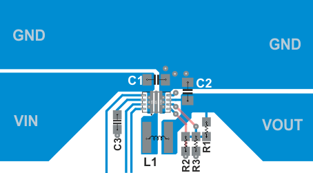
See Figure 81 for the recommended layout of the TPS62136x, which is designed for common external ground connections. The input capacitor should be placed as close as possible between the VIN and GND pin of TPS62136x. Also connect the VOS pin in the shortest way to VOUT at the output capacitor.
Provide low inductive and resistive paths for loops with high di/dt. Therefore paths conducting the switched load current should be as short and wide as possible. Provide low capacitive paths (with respect to all other nodes) for wires with high dv/dt. Therefore the input and output capacitance should be placed as close as possible to the IC pins and parallel wiring over long distances as well as narrow traces should be avoided. Loops which conduct an alternating current should outline an area as small as possible, as this area is proportional to the energy radiated.
Sensitive nodes like FB and VOS need to be connected with short wires and not nearby high dv/dt signals (for example SW). As they carry information about the output voltage, they should be connected as close as possible to the actual output voltage (at the output capacitor). The capacitor on the SS/TR pin as well as the FB resistors, R1 and R2, should be kept close to the IC and connect directly to those pins and the system ground plane. The same applies to R3 if FB2 is used to scale the output voltage.
The package uses the pins for power dissipation. Thermal vias on the VIN, GND and SW pins help to spread the heat through the pcb.
In case any of the digital inputs EN, VSEL or MODE need to be tied to the input supply voltage at VIN, the connection must be made directly at the input capacitor as indicated in the schematics.
The recommended layout is implemented on the EVM and shown in its User's Guide, SLVUAI7.
12.2 Layout Example
 Figure 81. Layout
12.3 Thermal Considerations
Implementation of integrated circuits in low-profile and fine-pitch surface-mount packages typically requires special attention to power dissipation. Many system-dependent issues such as thermal coupling, airflow, added heat sinks and convection surfaces, and the presence of other heat-generating components affect the power-dissipation limits of a given component.
Three basic approaches for enhancing thermal performance are listed below:
- Improving the power dissipation capability of the PCB design, for example, increasing copper thickness, thermal vias, number of layers
- Introducing airflow in the system
For more details on how to use the thermal parameters, see the application notes: Thermal Characteristics Application Note (SZZA017), and (SPRA953).
The TPS62136x is designed for a maximum operating junction temperature (TJ) of 125 °C. Therefore the maximum output power is limited by the power losses that can be dissipated over the actual thermal resistance, given by the package and the surrounding PCB structures. If the thermal resistance of the package is given, the size of the surrounding copper area and a proper thermal connection of the IC can reduce the thermal resistance. To get an improved thermal behavior, it's recommended to use top layer metal to connect the device with wide and thick metal lines. Internal ground layers can connect to vias directly under the IC for improved thermal performance.
If short circuit or overload conditions are present, the device is protected by limiting internal power dissipation.