SLVSC52B July 2013 – September 2015 TPS62152-Q1
PRODUCTION DATA.
- 1 Features
- 2 Applications
- 3 Description
- 4 Revision History
- 5 Pin Configuration and Functions
- 6 Specifications
-
7 Detailed Description
- 7.1 Overview
- 7.2 Functional Block Diagram
- 7.3
Feature Description
- 7.3.1 Pulse-Width Modulation (PWM) Operation
- 7.3.2 100% Duty-Cycle Operation
- 7.3.3 Enable / Shutdown (EN)
- 7.3.4 Soft Start or Tracking (SS/TR)
- 7.3.5 Current-Limit and Short-Circuit Protection
- 7.3.6 Power Good (PG)
- 7.3.7 Pin-Selectable Output Voltage (DEF)
- 7.3.8 Frequency Selection (FSW)
- 7.3.9 Undervoltage Lockout (UVLO)
- 7.3.10 Thermal Shutdown
- 7.3.11 Tracking Function
- 7.3.12 Feedback Pin (FB)
- 7.4 Device Functional Modes
- 8 Application and Implementation
- 9 Power Supply Recommendations
- 10Layout
- 11Device and Documentation Support
- 12Mechanical, Packaging, and Orderable Information
8 Application and Implementation
NOTE
Information in the following applications sections is not part of the TI component specification, and TI does not warrant its accuracy or completeness. TI’s customers are responsible for determining suitability of components for their purposes. Customers should validate and test their design implementation to confirm system functionality.
8.1 Application Information
The TPS62152-Q1 device is an automotive wide-input, synchronous step-down, DC-DC converter with a 3.3-V fixed output voltage and an output current of up to 1 A. The device can be used in buck-converter applications with an input range from 4 V to 17 V. The TPS62152-Q1 device is optimized for space constrained applications and consumes 17-µA (typical) current in power-save mode. Selectable switching frequency (1.25 MHz or 2.25 MHz) allows regulator design to be optimized for efficiency or solution size.
8.2 Typical Application
 Figure 28. 3.3-V, 1-A Power Supply
8.2.1 Design Requirements
The device is optimized for a certain range of output inductor and output capacitor values. See the Detailed Design Procedure section for details. The Recommended Operating Conditions table lists the allowed ranges for the input voltage, input buffer capacitor, output inductor, and output buffer capacitor. The values listed in this table must be followed when designing the regulator. Low-ESR ceramic capacitors should be used at the input and output for better filtering and ripple performance. The Detailed Design Procedure section provides the necessary equations and guidelines for selecting external components for this regulator.
8.2.2 Detailed Design Procedure
8.2.2.1 External Component Selection
The external components must fulfill the needs of the application, but also the stability criteria of the device control loop. Table 2 lists recommended components based on the schematic in Figure 28.
Table 2. List of Components
| REFERENCE | DESCRIPTION | MANUFACTURER |
|---|---|---|
| IC | 17-V, 1-A step-down converter, VQFN | TPS62152-Q1 RGT, Texas Instruments |
| LOUT | Inductor, 2.2-µH, 3.1-A, 0.165 in × 0.165 in (4,24 cm × 4,24 cm) | XFL4020-222MEB, Coilcraft |
| CIN | Capacitor, 10-µF, 25-V, ceramic | Standard |
| COUT | Capacitor, 22-µF, 6.3-V, ceramic | Standard |
| CSS | Capacitor, 3300-pF, 25-V, ceramic | |
| RPG | Resistor, 100 kΩ, chip, 0603, 1/16 W, 1% | Standard |
The TPS62152-Q1 works optimally within a range of external components. Consider the inductance and capacitance if the LC output filter in conjunction so as to create a double pole, responsible for the corner frequency of the converter (see the Output Filter and Loop Stability section). Use Table 3 to simplify the output-filter component selection.
Table 3. L-C Output Filter Combinations(1)
| 10 µF | 22 µF | 47 µF | 100 µF | 200 µF | |
|---|---|---|---|---|---|
| 1 µH | √ | √ | √ | √ | |
| 2.2 µH | √ | √(2) | √ | √ | √ |
| 3.3 µH | √ | √ | √ | √ |
The TPS62152-Q1 device can run with an inductor as low as 1 µH or 2.2 µH for the high-frequency setting (FSW = Low). However, for applications running with the low-frequency setting (FSW = High) or with low input voltages, 3.3 µH is a better recommendation. See Optimizing the TPS62130/40/50/60/70 Output Filter, SLVA463, for detailed information on further LC combinations.
8.2.2.1.1 Inductor Selection
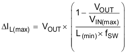
Several effects like inductor ripple current, output ripple voltage, PWM-to-PSM transition point and efficiency affect the inductor selection. In addition, the inductor selected require rating for appropriate saturation current and dc resistance (DCR). Equation 7 and Equation 8 calculate the maximum inductor current under static load conditions.

where
- IL(max) is the maximum inductor current.
where
- L(min) is the minimum effective inductor value.
- fSW is the actual PWM switching frequency.
Calculating the maximum inductor current using the actual operating conditions gives the minimum required saturation current of the inductor. TI recommends adding a margin of about 20%. A larger inductor value is also useful to achieve lower ripple current, but increases the transient response time and may require a larger package. TI recommends the inductors listed in Table 4, which have worked successfully with the TPS62152-Q1.
Table 4. List of Inductors
| TYPE | INDUCTANCE [µH] |
SATURATION CURRENT [A](1) |
DIMENSIONS [L × W × H, mm] |
MANUFACTURER |
|---|---|---|---|---|
| XFL4020-222ME_ | 2.2 µH, ±20% | 3.5 | 4 × 4 × 2.1 | Coilcraft |
| XFL3012-222MEC | 2.2 µH, ±20% | 1.6 | 3 × 3 × 1.2 | Coilcraft |
| XFL3012-332MEC | 3.3 µH, ±20% | 1.4 | 3 × 3 × 1.2 | Coilcraft |
| VLS252012T-2R2M1R3 | 2.2 µH, ±20% | 1.3 | 2.5 × 2 × 1.2 | TDK |
| LPS3015-332 | 3.3 µH, ±20% | 1.4 | 3 × 3 × 1.4 | Coilcraft |
| 744025003 | 3.3 µH, ±20% | 1.5 | 2.8 × 2.8 × 2.8 | Wuerth |
| PSI25201B-2R2MS | 2.2 µH, ±20% | 1.3 | 2 × 2.5 × 1.2 | Cyntec |
| NR3015T-2R2M | 2.2 µH, ±20% | 1.5 | 3 × 3 × 1.5 | Taiyo Yuden |
The inductor value also determines the load current at which the device enters power-save mode as shown in Equation 9.

The designer can use Equation 8 to calculate the inductor value for changing this current level.
8.2.2.1.2 Output Capacitor
The recommended value for the output capacitor is 22 µF. The architecture of the TPS62152-Q1 device allows the use of ceramic output capacitors with low equivalent series resistance (ESR). These capacitors provide low output-voltage ripple and are ideal. To keep low resistance up to high frequencies and to get narrow capacitance variation with temperature, TI recommends using X7R or X5R dielectric. Using a higher value can have some advantages, such as smaller voltage ripple and a tighter DC output accuracy in power-save mode (see SLVA463).
NOTE
In power-save mode, the output-voltage ripple depends on the output capacitance and the ESR and peak inductor current of the capacitor. Using ceramic capacitors provides low ESR and low ripple.
8.2.2.1.2.1 Input Capacitor
For most applications, 10 µF is sufficient and recommended, though a larger value reduces input current ripple further. The input capacitor buffers the input voltage for transient events and also decouples the converter from the supply. TI recommends low-ESR multilayer ceramic capacitor for best filtering. Place the capacitor between PVIN and PGND as close as possible to those pins. Even though the AVIN and PVIN supply must come from the same input source, it is a good idea to place a capacitance of 0.1 µF from AVIN to AGND, to avoid potential noise coupling. Use of an RC low-pass filter from PVIN to AVIN is allowable but not mandatory.
8.2.2.1.2.2 Soft-Start Capacitor
A capacitance connected between SS/TR pin and AGND allows a user-programmable start-up slope of the output voltage. A constant-current source provides 2.5 µA to charge the external capacitance. Use Equation 10 to calculate the capacitance required for a given soft-start ramp time for the output voltage.

where
- CSS is the capacitance (F) required at the SS/TR pin
- tSS is the desired soft-start ramp time (s).
NOTE
DC bias effect: High-capacitance ceramic capacitors have a DC bias effect, which has a strong influence on the final effective capacitance. Therefore, choose the right capacitor value carefully. Package size and voltage rating in combination with dielectric material are responsible for differences between the rated capacitor value and the effective capacitance.
8.2.2.2 Output Filter and Loop Stability
The TPS62152-Q1 device has internal compensation to be stable with L-C filter combinations corresponding to a corner frequency calculated with Equation 11.

Table 3 gives proven and recommended nominal values for inductance and ceramic capacitance. Different values may work, but take care not to affect the loop stability. See Optimizing the TPS62130/40/50/60/70 Output Filter, SLVA463, for more information, including a detailed L-C stability matrix.
The TPS62152-Q1 device includes an internal 25-pF feedforward capacitor, connected between the VOS and FB pins. This capacitor impacts the frequency behavior and sets a pole and zero in the control loop with the resistors of the feedback divider, according to equations Equation 12 and Equation 13.


Though the TPS62152-Q1 device is stable without the pole and zero being in a particular location, adjusting their location to the specific needs of the application can provide better performance in power-save mode and/or improved transient response. An external feedforward capacitor can also be added. The application reports Optimizing Transient Response of Internally Compensated dc-dc Converters With Feedforward Capacitor, SLVA289, and Using a Feedforward Capacitor to Improve Stability and Bandwidth of TPS62130/40/50/60/70, SLVA466, provide a more-detailed discussion on the optimization for stability vs transient response.
8.2.3 Application Curves
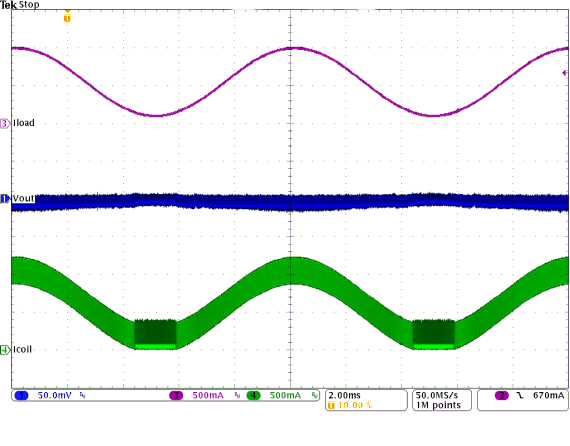 Figure 29. PWM-PSM-Transition
for VIN = 12 V With 50 mV/div
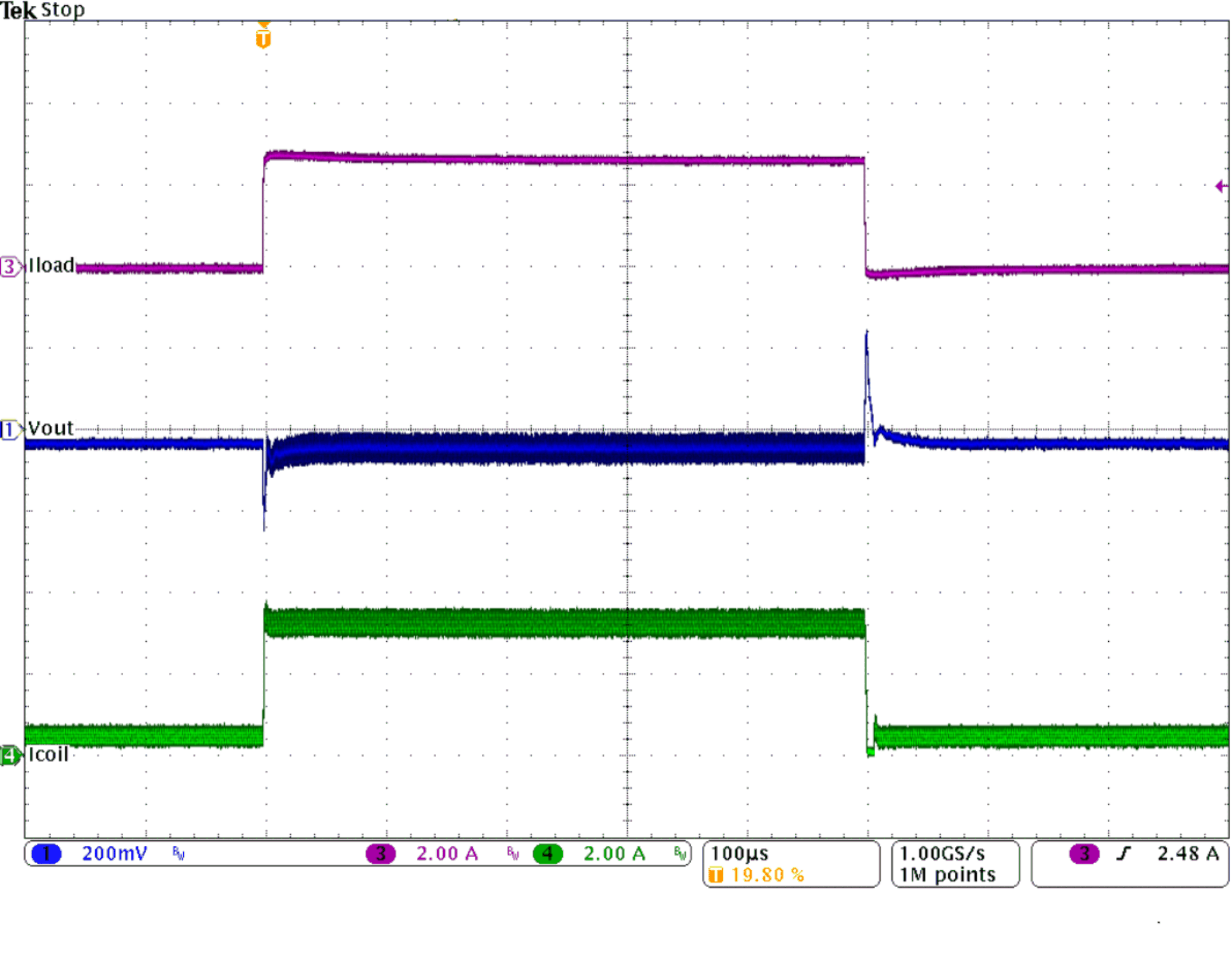 Figure 30. Load Transient Response for VIN = 12 V and
IOUT= 0 A to 2.5 A and back to 0 A
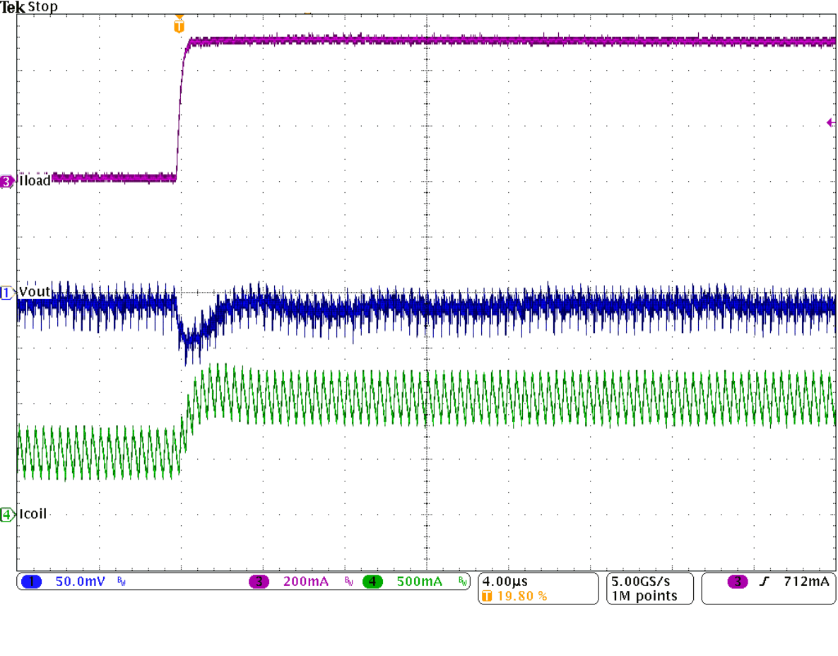 Figure 31. Load Transient Response of Figure 30,
Rising Edge
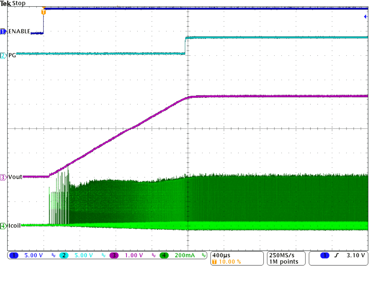 Figure 33. Startup into 100 mA for VIN = 12 V
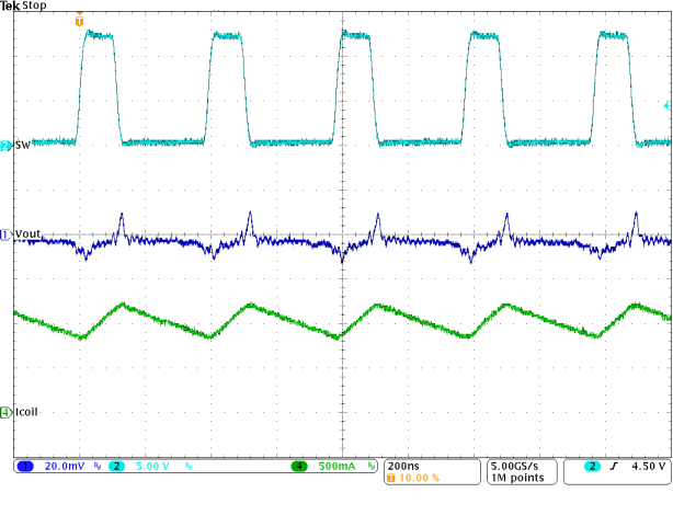 Figure 35. Typical Operation in PWM Mode With IOUT = 1 A
 Figure 32. Load Transient Response of Figure 30,
Falling Edge
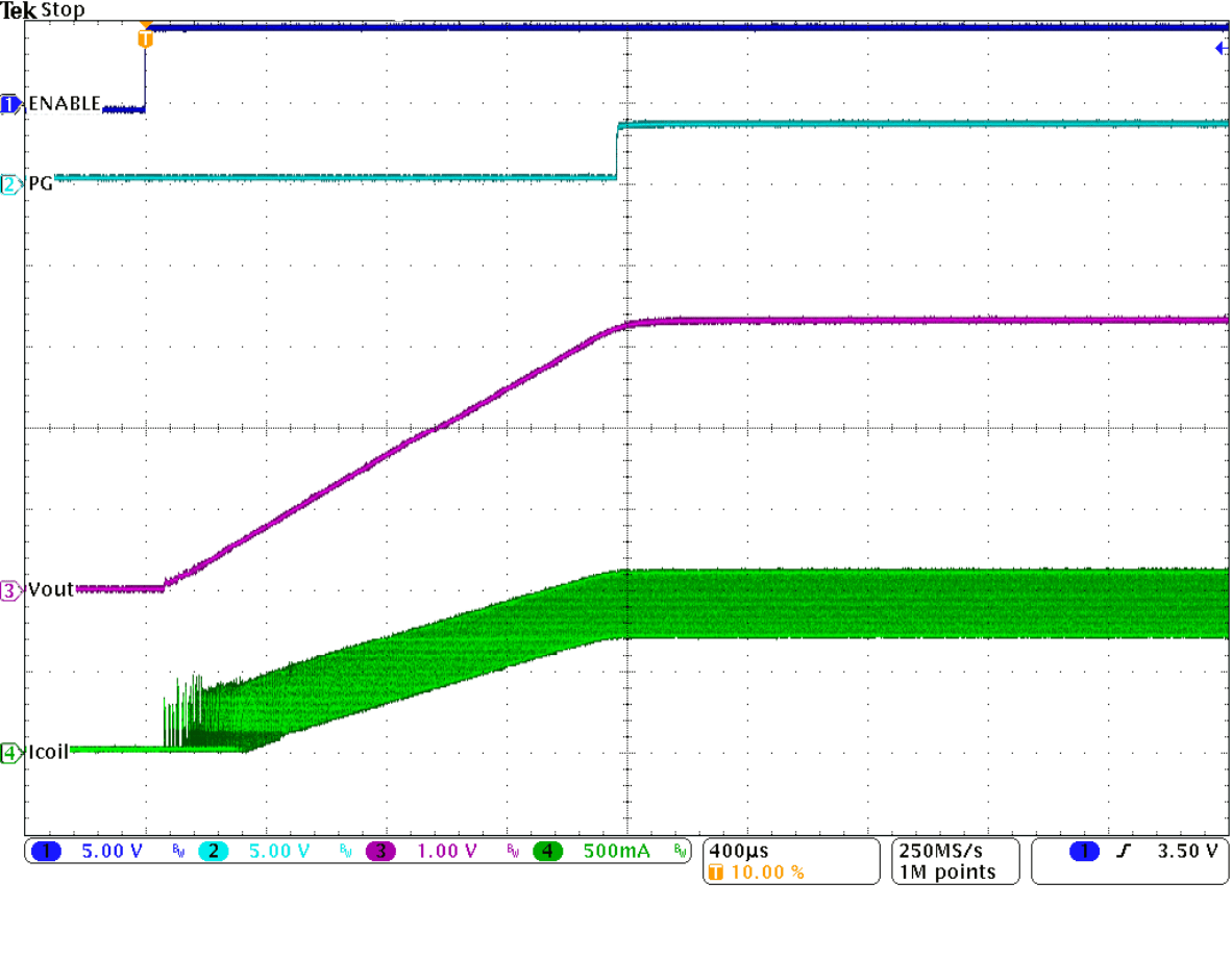 Figure 34. Startup into 1 A for VIN = 12 V
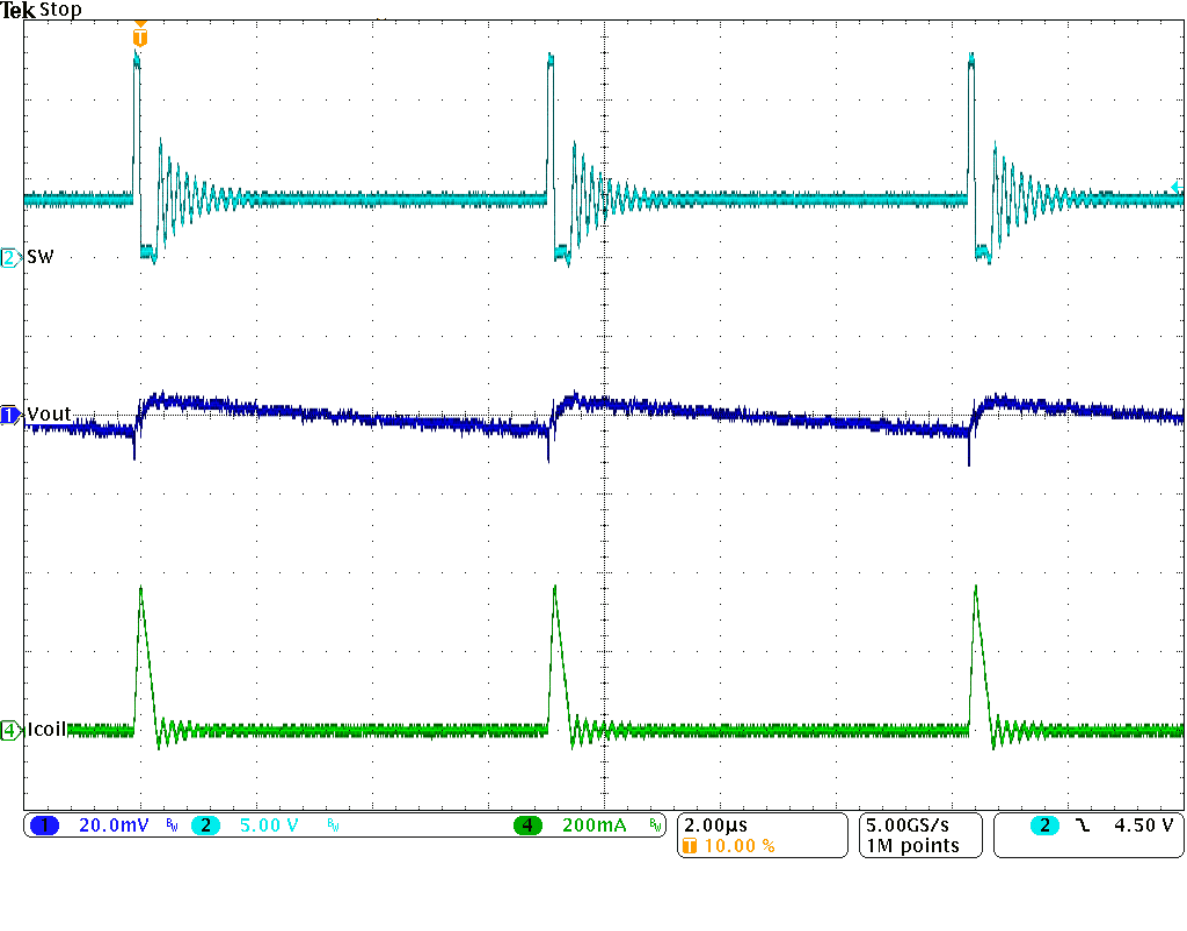 Figure 36. Typical Operation in Power Save Mode
With IOUT = 10 mA