SLVSC52B July 2013 – September 2015 TPS62152-Q1
PRODUCTION DATA.
- 1 Features
- 2 Applications
- 3 Description
- 4 Revision History
- 5 Pin Configuration and Functions
- 6 Specifications
-
7 Detailed Description
- 7.1 Overview
- 7.2 Functional Block Diagram
- 7.3
Feature Description
- 7.3.1 Pulse-Width Modulation (PWM) Operation
- 7.3.2 100% Duty-Cycle Operation
- 7.3.3 Enable / Shutdown (EN)
- 7.3.4 Soft Start or Tracking (SS/TR)
- 7.3.5 Current-Limit and Short-Circuit Protection
- 7.3.6 Power Good (PG)
- 7.3.7 Pin-Selectable Output Voltage (DEF)
- 7.3.8 Frequency Selection (FSW)
- 7.3.9 Undervoltage Lockout (UVLO)
- 7.3.10 Thermal Shutdown
- 7.3.11 Tracking Function
- 7.3.12 Feedback Pin (FB)
- 7.4 Device Functional Modes
- 8 Application and Implementation
- 9 Power Supply Recommendations
- 10Layout
- 11Device and Documentation Support
- 12Mechanical, Packaging, and Orderable Information
6 Specifications
6.1 Absolute Maximum Ratings
over operating free-air temperature range (unless otherwise noted)(1)| MIN | MAX | UNIT | ||
|---|---|---|---|---|
| Pin voltage range(2) | AVIN, PVIN | –0.3 | 20 | V |
| EN, SS/TR | –0.3 | VIN + 0.3 | ||
| SW | –0.3 | VIN + 0.3 | ||
| DEF, FSW, FB, PG, VOS | –0.3 | 7 | ||
| Power-good sink current | PG | 10 | mA | |
| Operating junction temperature, TJ | –40 | 125 | °C | |
| Storage temperature, Tstg | –65 | 150 | °C | |
(1) Stresses beyond those listed under Absolute Maximum Ratings may cause permanent damage to the device. These are stress ratings only, which do not imply functional operation of the device at these or any other conditions beyond those indicated under Recommended Operating Conditions. Exposure to absolute-maximum-rated conditions for extended periods may affect device reliability.
(2) All voltages are with respect to network ground terminal.
6.2 ESD Ratings
| VALUE | UNIT | ||||
|---|---|---|---|---|---|
| V(ESD) | Electrostatic discharge | Human body model (HBM), per AEC Q100-002(1) | ±2000 | V | |
| Charged device model (CDM), per AEC Q100-011 | All pins | ±500 | |||
| Corner pins (1, 4, 5, 8, 9, 12, 13, 16) | ±750 | ||||
(1) AEC Q100-002 indicates HBM stressing is done in accordance with the ANSI/ESDA/JEDEC JS-001 specification.
6.3 Recommended Operating Conditions
over operating free-air temperature range (unless otherwise noted)| MIN | MAX | UNIT | |||
|---|---|---|---|---|---|
| VIN | Supply voltage at AVIN and PVIN(1) | 4 | 17 | V | |
| CIN | Input filter capacitor | 10 | µF | ||
| COUT | Output buffer capacitor | 10 | µF | ||
| LOUT | Output inductor | 1 | 3.3 | µH | |
| TA | Operating free air temperature | –40 | 125 | °C | |
(1) The device is still functional down to the undervoltage lockout (see the VUVLO parameter in the Electrical Characteristics table).
6.4 Thermal Information
| THERMAL METRIC(1) | TPS62152-Q1 | UNIT | |
|---|---|---|---|
| RGT (VQFN) | |||
| 16 Pins | |||
| RθJA | Junction-to-ambient thermal resistance | 45 | °C/W |
| RθJC(top) | Junction-to-case (top) thermal resistance | 51.6 | °C/W |
| RθJB | Junction-to-board thermal resistance | 17.4 | °C/W |
| ψJT | Junction-to-top characterization parameter | 0.9 | °C/W |
| ψJB | Junction-to-board characterization parameter | 17.4 | °C/W |
| RθJC(bot) | Junction-to-case (bottom) thermal resistance | 4.4 | °C/W |
(1) For more information about traditional and new thermal metrics, see the Semiconductor and IC Package Thermal Metrics application report, SPRA953.
6.5 Electrical Characteristics
over free-air temperature range (TA= –40°C to 125°C), typical values at VIN = AVIN = PVIN = 12 V and TA = 25°C (unless otherwise noted)| PARAMETER | TEST CONDITIONS | MIN | TYP | MAX | UNIT | ||
|---|---|---|---|---|---|---|---|
| SUPPLY | |||||||
| VIN | Input voltage range(1) | 4 | 17 | V | |||
| IQ | Operating quiescent current | EN = High, IOUT = 0 mA, device not switching | 17 | 25 | µA | ||
| ISD | Shutdown current(2) | EN = Low | 1.5 | 4 | µA | ||
| VUVLO | Undervoltage lockout threshold | Falling input voltage | 2.6 | 2.7 | 2.8 | V | |
| Hysteresis | 200 | mV | |||||
| TSD | Thermal shutdown temperature | 160 | °C | ||||
| Thermal shutdown hysteresis | 20 | °C | |||||
| CONTROL (EN, DEF, FSW, SS/TR, PG) | |||||||
| VH | High-level input threshold voltage (EN, DEF, FSW) | 0.9 | V | ||||
| VL | Low-level input threshold voltage (EN, DEF, FSW) | 0.3 | V | ||||
| ILKG | Input leakage current (EN, DEF, FSW) | EN = VIN or GND; DEF, FSW = VOUT or GND | 0.01 | 1 | µA | ||
| VTH_PG | Power-good threshold voltage | Rising (%VOUT) | 92% | 95% | 98% | ||
| Falling (%VOUT) | 87% | 90% | 94% | ||||
| VOL_PG | Power-good output low | IPG = –2 mA | 0.07 | 0.3 | V | ||
| ILKG_PG | Input leakage current (PG) | VPG = 1.8 V | 1 | 400 | nA | ||
| ISS/TR | SS/TR pin source current | 2.3 | 2.5 | 2.7 | µA | ||
| POWER SWITCH | |||||||
| RDS(ON) | High-side MOSFET on-resistance | VIN ≥ 6 V | 90 | 170 | mΩ | ||
| VIN = 3 V | 120 | ||||||
| Low-side MOSFET on-resistance | VIN ≥ 6 V | 40 | 70 | ||||
| VIN = 3 V | 50 | ||||||
| ILIMF | High-side MOSFET forward current limit(3) | VIN = 12 V, TA= 25°C | 1.4 | 1.7 | 2.2 | A | |
| OUTPUT | |||||||
| VREF | Internal reference voltage(4) | 0.8 | V | ||||
| ILKG_FB | Input leakage current (FB) | VFB = 0.8 V | 1 | 100 | nA | ||
| VOUT | Output voltage range | VIN ≥ VOUT | 3.3 | V | |||
| DEF (Output voltage programming) | DEF = 0 (GND) | VOUT | V | ||||
| DEF = 1 (VOUT) | VOUT + 5% | ||||||
| Initial output voltage accuracy(5) | PWM mode operation, VIN ≥ VOUT + 1 V | –1.8% | 1.8% | ||||
| Power-save mode operation, COUT = 22 µF | –2.3% | 2.8% | |||||
| Load regulation(6) | VIN = 12 V, VOUT = 3.3 V, PWM mode operation | 0.05 | %/A | ||||
| Line regulation(6) | 3 V ≤ VIN ≤ 17 V, VOUT = 3.3 V, IOUT = 1 A, PWM mode operation | 0.02 | %/V | ||||
(1) The device is still functional down to undervoltage lockout (see parameter VUVLO).
(2) Current into AVIN + PVIN pin
(3) This is the static current limit. It can be temporarily higher in applications because of internal propagation delay (see Current-Limit and Short-Circuit Protection section).
(4) This is the voltage regulated at the FB pin.
(5) This is the accuracy provided by the device itself (line and load regulation effects are not included). The (internal) resistive divider is included.
6.6 Typical Characteristics
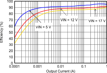
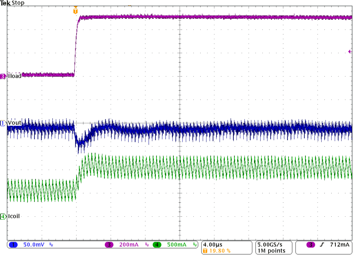
Table 1. Table of Graphs
| DESCRIPTION | FIGURE | ||
|---|---|---|---|
| Efficiency | vs Output Current | Figure 1, Figure 3 | |
| vs Input Voltage | Figure 2, Figure 4 | ||
| Output Voltage Accuracy | Load Regulation | Figure 5 | |
| Line Regulation | Figure 6 | ||
| Switching Frequency | vs Input Voltage | Figure 7 | |
| vs Output Current | Figure 8 | ||
| Input Quiescent Current | vs Input voltage | Figure 9 | |
| Input Shutdown Current | vs Input voltage | Figure 10 | |
| High-Side Static Drain-Source-Resistance (RDSon) | vs Input voltage | Figure 11 | |
| Low-Side Static Drain-Source-Resistance (RDSon) | vs Input voltage | Figure 12 | |
| Output Voltage Ripple | vs Output Current | Figure 13 | |
| Output Current | vs Input Voltage | Figure 14 | |
| Power-Supply Rejection Ratio | vs Frequency | Figure 15, Figure 16 | |
| PWM-PSM-Transition | Figure 17 | ||
| Load Transient Response | Figure 18 | ||
| Load Transient Response | Rising Edge | Figure 19 | |
| Falling Edge | Figure 20 | ||
| Startup | Into 100 mA | Figure 21 | |
| Into 1 A | Figure 22 | ||
| Typical Operation in PWM Mode | Figure 23 | ||
| Typical Operation in Power Save Mode | Figure 24 | ||

| FSW = 1.25 MHz | L = 2.2 µH (XFL4020) | COUT = 22 µF |
| CIN = 10 µF |
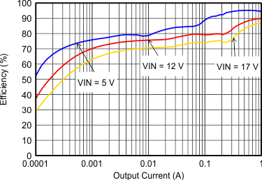
| FSW = 2.5 MHz | L = 2.2 µH (XFL4020) | COUT = 22 µF |
| CIN = 10 µF |
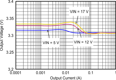
| L = 2.2 µH (XFL4020) | COUT = 22 µF | CIN = 10 µF |
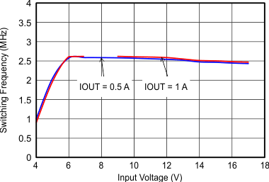
| L = 2.2 µH (XFL4020) | COUT = 22 µF | CIN = 10 µF |
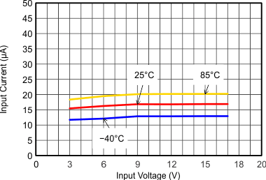
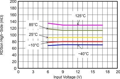
vs Input Voltage
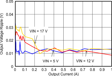
| L = 2.2 µH (XFL4020) | COUT = 22 µF | CIN = 10 µF |
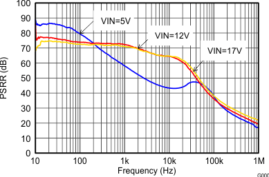
| FSW = 2.5 MHz | L = 2.2 µH (XFL4020) | COUT = 22 µF |
| CIN = 10 µF |
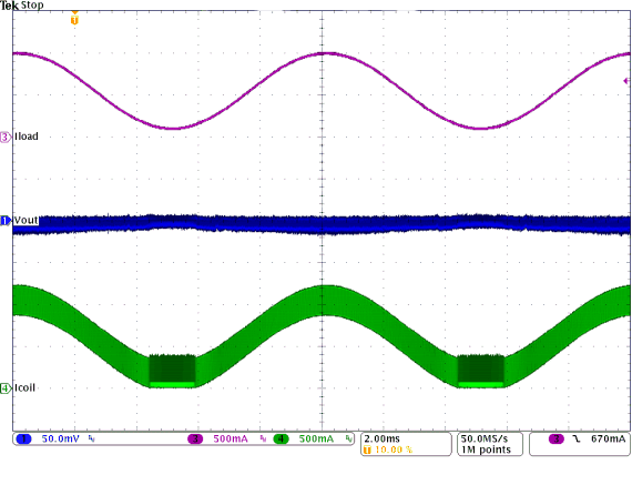
| VIN = 12 V With 50 mV/div | ||
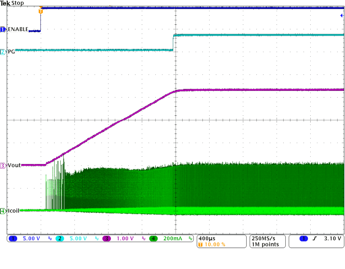
| VIN = 12 V | ||
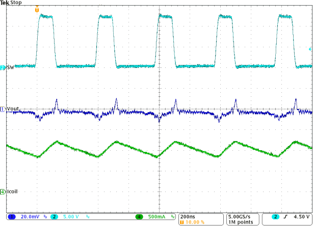
| IOUT = 1 A |
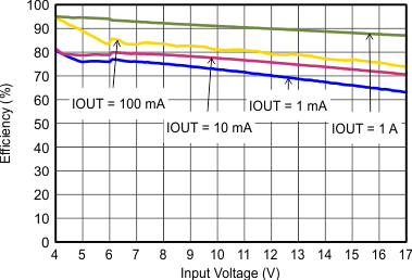
| FSW = 2.5 MHz | L = 2.2 µH (XFL4020) | COUT = 22 µF |
| CIN = 10 µF |
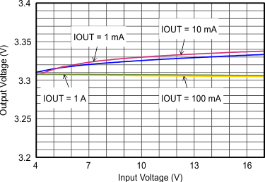
| L = 2.2 µH (XFL4020) | COUT = 22 µF | CIN = 10 µF |
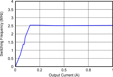
| FSW = Low | L = 2.2 µH (XFL4020) | COUT = 22 µF |
| CIN = 10 µF |
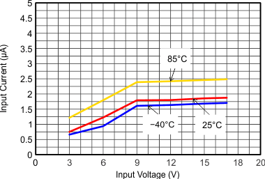
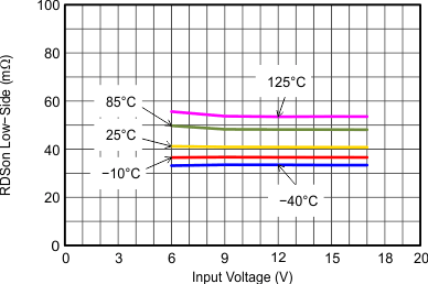
vs Input Voltage
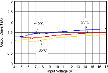
| L = 2.2 µH (XFL4020) | COUT = 22 µF | CIN = 10 µF |
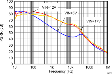
| FSW = 2.5 MHz | L = 2.2 µH (XFL4020) | COUT = 22 µF |
| CIN = 10 µF |
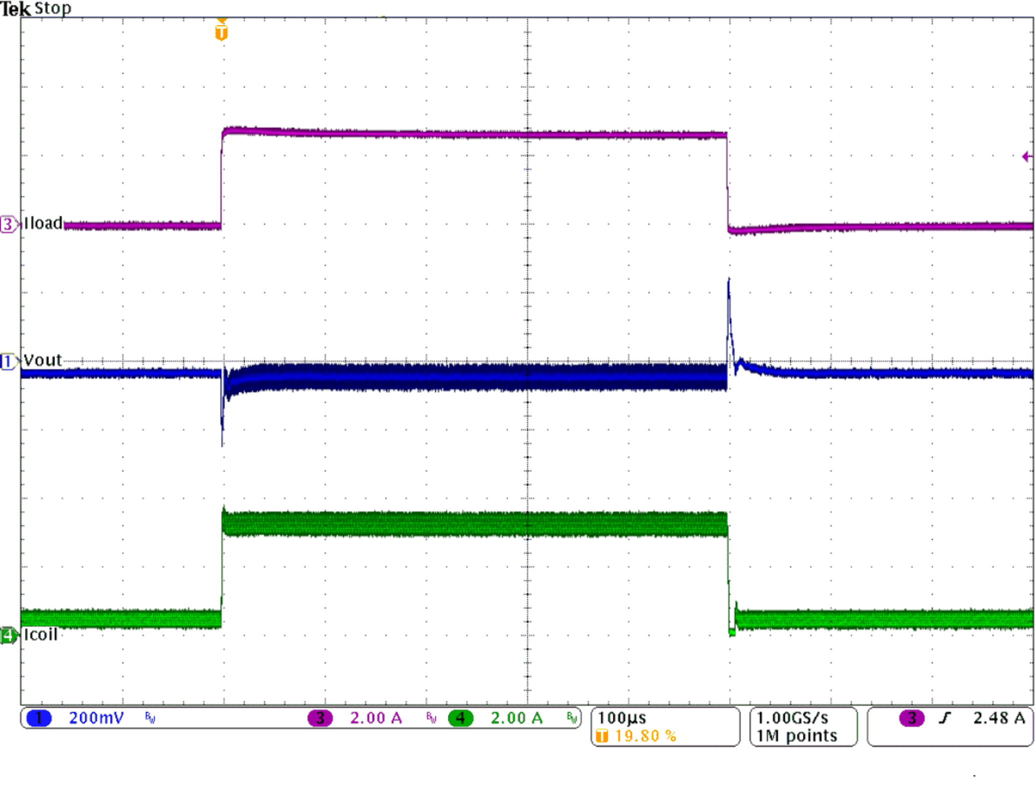
| VIN = 12 V | IOUT = 0 to 5 A and back to 0 A | |
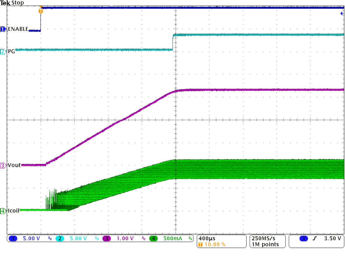
| VIN = 12 V | ||
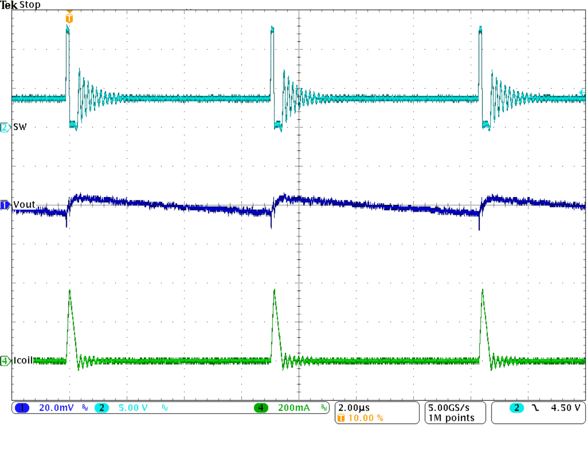
| IOUT = 10 mA |
