ZHCSCG9C May   2014  – July 2019 TPS62150A-Q1 , TPS62152A-Q1 , TPS62153A-Q1

PRODUCTION DATA.  

  1. 特性
  2. 应用
  3. 说明
    1.     Device Images
      1.      典型应用电路原理图 空白 空白 空白
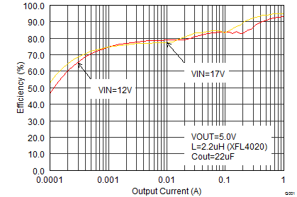
      2.      效率与输出电流 空白
  4. 修订历史记录
  5. Device Comparison Table
  6. Pin Configuration and Functions
    1.     Pin Functions
  7. Specifications
    1. 7.1 Absolute Maximum Ratings
    2. 7.2 Handling Ratings
    3. 7.3 Recommended Operating Conditions
    4. 7.4 Thermal Information
    5. 7.5 Electrical Characteristics
    6. 7.6 Typical Characteristics
  8. Parameter Measurement Information
  9. Detailed Description
    1. 9.1 Overview
    2. 9.2 Functional Block Diagram
    3. 9.3 Feature Description
      1. 9.3.1  Pulse Width Modulation (PWM) Operation
      2. 9.3.2  Power Save Mode Operation
      3. 9.3.3  100% Duty-Cycle Operation
      4. 9.3.4  Enable / Shutdown (EN)
      5. 9.3.5  Soft Start / Tracking (SS/TR)
      6. 9.3.6  Current Limit And Short Circuit Protection
      7. 9.3.7  Power Good (PG)
      8. 9.3.8  Pin-Selectable Output Voltage (DEF)
      9. 9.3.9  Frequency Selection (FSW)
      10. 9.3.10 Under Voltage Lockout (UVLO)
      11. 9.3.11 Thermal Shutdown
    4. 9.4 Device Functional Modes
      1. 9.4.1 Operation above TJ=125°C
      2. 9.4.2 Operation with VIN < 3V
      3. 9.4.3 Operation with separate EN Control
  10. 10Application and Implementation
    1. 10.1 Application Information
    2. 10.2 Typical Application
      1. 10.2.1 TPS62150A-Q1 Point-Of-Load Step Down Converter
        1. 10.2.1.1 Design Requirements
        2. 10.2.1.2 Detailed Design Procedure
          1. 10.2.1.2.1 Custom Design With WEBENCH® Tools
          2. 10.2.1.2.2 Programming The Output Voltage
          3. 10.2.1.2.3 External Component Selection
          4. 10.2.1.2.4 Inductor Selection
          5. 10.2.1.2.5 Output Capacitor
          6. 10.2.1.2.6 Input Capacitor
          7. 10.2.1.2.7 Soft Start Capacitor
          8. 10.2.1.2.8 Tracking Function
          9. 10.2.1.2.9 Output Filter And Loop Stability
        3. 10.2.1.3 Application Curves
      2. 10.2.2 System Examples
        1. 10.2.2.1 Regulated Power LED Supply
        2. 10.2.2.2 Inverting Power Supply
        3. 10.2.2.3 Active Output Discharge
        4. 10.2.2.4 Various Output Voltages
  11. 11Power Supply Recommendations
  12. 12Layout
    1. 12.1 Layout Guidelines
    2. 12.2 Layout Example
  13. 13器件和文档支持
    1. 13.1 器件支持
      1. 13.1.1 第三方米6体育平台手机版_好二三四免责声明
    2. 13.2 相关链接
    3. 13.3 接收文档更新通知
    4. 13.4 社区资源
    5. 13.5 商标
    6. 13.6 静电放电警告
    7. 13.7 Glossary
  14. 14机械、封装和可订购信息

封装选项

请参考 PDF 数据表获取器件具体的封装图。

机械数据 (封装 | 引脚)
  • RGT|16
散热焊盘机械数据 (封装 | 引脚)
订购信息

Application Curves

At VIN=12V, VOUT=3.3V and TA=25°C, FSW=Low, (unless otherwise noted)
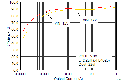
TPS62150A-Q1 TPS62152A-Q1 TPS62153A-Q1 SLVSCC3_eff50ioutfull.png
FSW = Low
Figure 12. Efficiency vs. Output Current
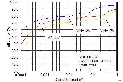
TPS62150A-Q1 TPS62152A-Q1 TPS62153A-Q1 SLVSCC3_eff50iouthalf.png
FSW = High
Figure 14. Efficiency vs. Output Current
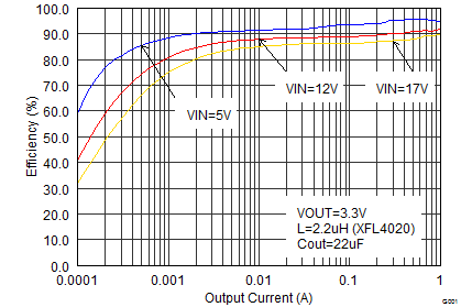
TPS62150A-Q1 TPS62152A-Q1 TPS62153A-Q1 SLVSCC3_eff33ioutfull.png
FSW = Low
Figure 16. Efficiency vs. Output Current
TPS62150A-Q1 TPS62152A-Q1 TPS62153A-Q1 SLVSCC3_eff33iouthalf.png
FSW = High
Figure 18. Efficiency vs. Output Current
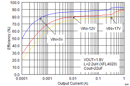
TPS62150A-Q1 TPS62152A-Q1 TPS62153A-Q1 SLVSCC3_eff18iouthalf.png
FSW = High
Figure 20. Efficiency vs. Output Current
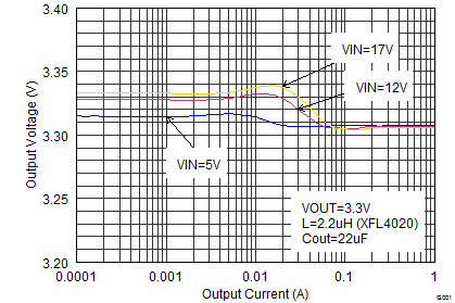
TPS62150A-Q1 TPS62152A-Q1 TPS62153A-Q1 SLVSCC3_loadreg.png
VOUT = 3.3 V L = 2.2 µH (XFL4020) COUT = 22 µF
Figure 22. Output Voltage Accuracy (Load Regulation)
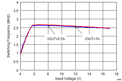
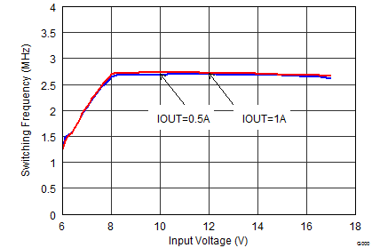
TPS62150A-Q1 TPS62152A-Q1 TPS62153A-Q1 SLVSAL5_fswvin_5.0V.png
FSW = Low VOUT = 5 V
Figure 24. Switching Frequency vs Input Voltage
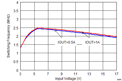
TPS62150A-Q1 TPS62152A-Q1 TPS62153A-Q1 SLVSAL5_fswvin_3.3V.png
FSW = Low VOUT = 3.3 V
Figure 26. Switching Frequency vs Input Voltage
TPS62150A-Q1 TPS62152A-Q1 TPS62153A-Q1 SLVSAL5_fswvin_1.8V.png
FSW = Low VOUT = 1.8 V
Figure 28. Switching Frequency vs Input Voltage
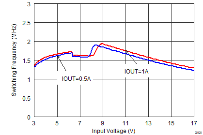
TPS62150A-Q1 TPS62152A-Q1 TPS62153A-Q1 SLVSAL5_fswvin_1.0V.png
FSW = Low VOUT = 1 V
Figure 30. Switching Frequency vs Input Voltage
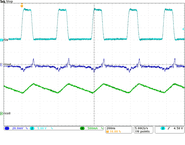
TPS62150A-Q1 TPS62152A-Q1 TPS62153A-Q1 SLVSCC3_PWMtyp.gifFigure 32. Typical Operation in PWM Mode (IOUT = 1A)
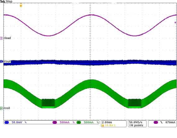
TPS62150A-Q1 TPS62152A-Q1 TPS62153A-Q1 SLVSCC3_modetran.gifFigure 34. PWM-PSM-Transition
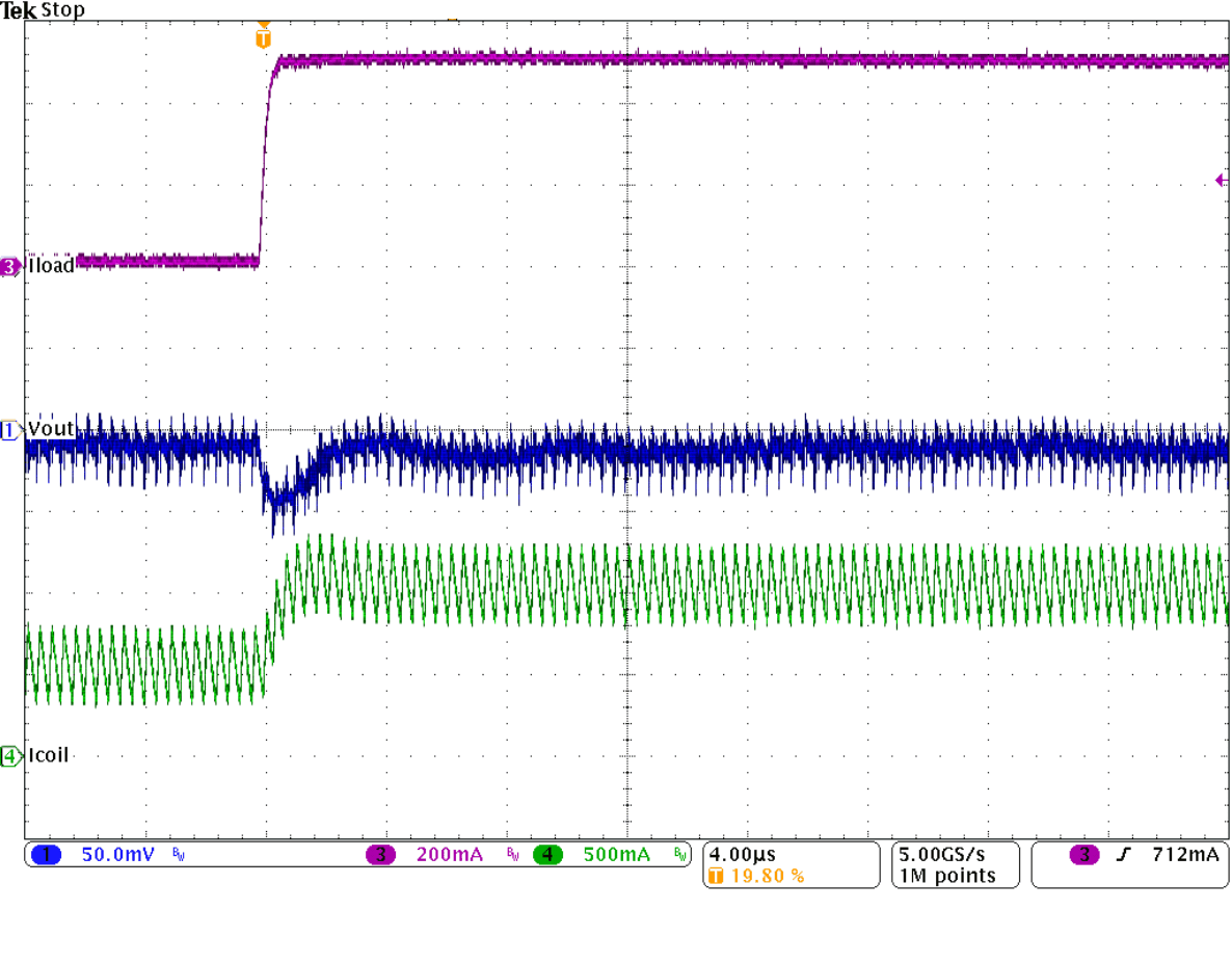
TPS62150A-Q1 TPS62152A-Q1 TPS62153A-Q1 SLVSCC3_loadtranrise.gifFigure 36. Load Transient Response of Figure 35,
Rising Edge
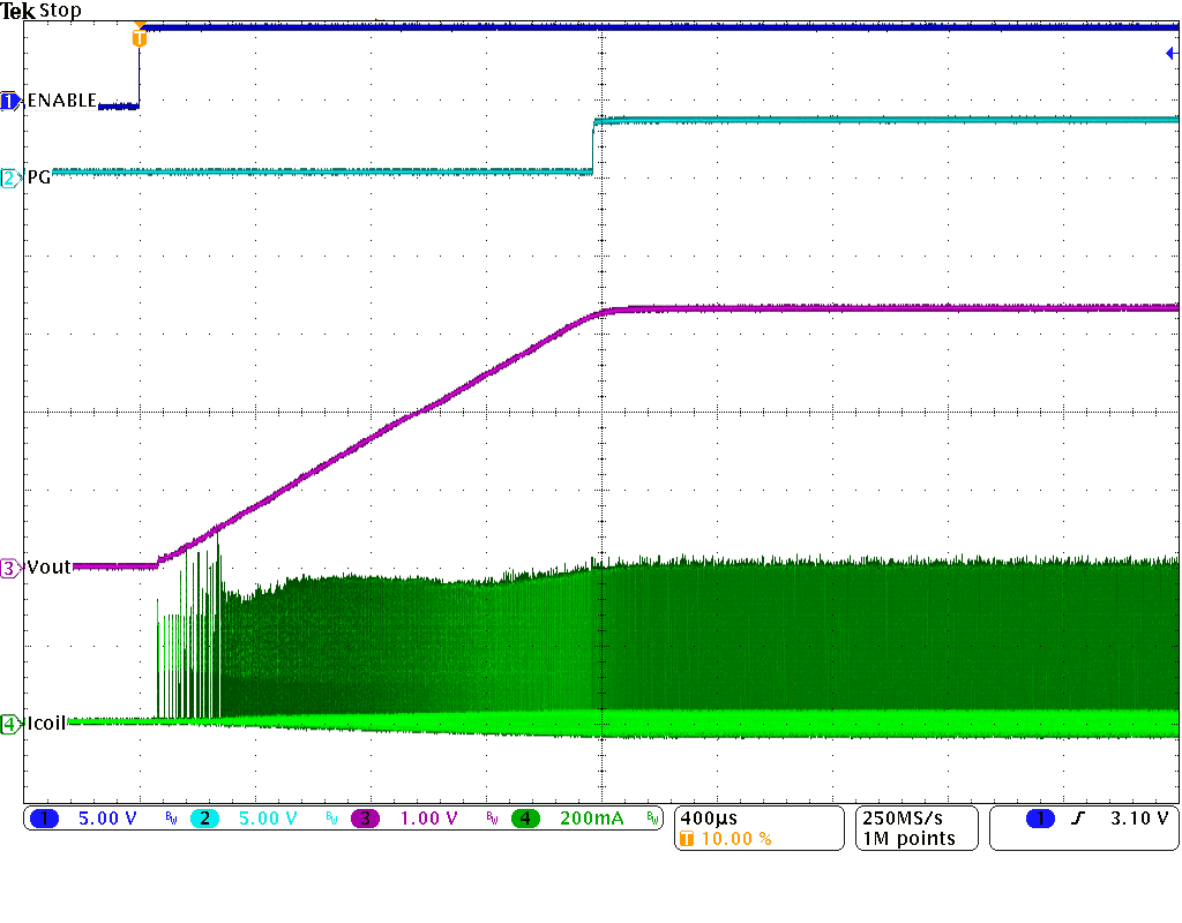
TPS62150A-Q1 TPS62152A-Q1 TPS62153A-Q1 SLVSCC3_stuplow.gifFigure 38. Start Up Into 100mA
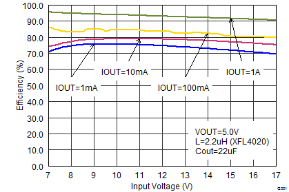
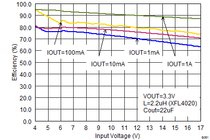
TPS62150A-Q1 TPS62152A-Q1 TPS62153A-Q1 SLVSCC3_eff50vinfull.png
FSW = Low
Figure 13. Efficiency vs. Input Voltage
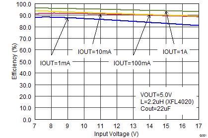
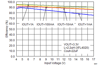
TPS62150A-Q1 TPS62152A-Q1 TPS62153A-Q1 SLVSCC3_eff50vinhalf.png
FSW = High
Figure 15. Efficiency vs. Input Voltage
TPS62150A-Q1 TPS62152A-Q1 TPS62153A-Q1 SLVSCC3_eff33vinfull.png
FSW = Low
Figure 17. Efficiency vs. Input Voltage
TPS62150A-Q1 TPS62152A-Q1 TPS62153A-Q1 SLVSCC3_eff33vinhalf.png
FSW = High
Figure 19. Efficiency vs. Input Voltage
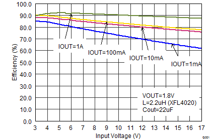
TPS62150A-Q1 TPS62152A-Q1 TPS62153A-Q1 SLVSCC3_eff18vinhalf.png
FSW = High
Figure 21. Efficiency vs. Input Voltage
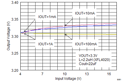
TPS62150A-Q1 TPS62152A-Q1 TPS62153A-Q1 SLVSCC3_linereg.png
VOUT = 3.3 V L = 2.2 µH (XFL4020) COUT = 22 µF
Figure 23. Output Voltage Accuracy (Line Regulation)
TPS62150A-Q1 TPS62152A-Q1 TPS62153A-Q1 SLVSAL5_fswiout_5.0V.png
FSW = Low VOUT = 5 V
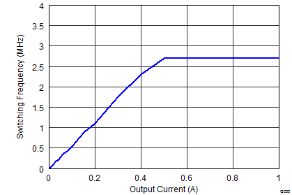
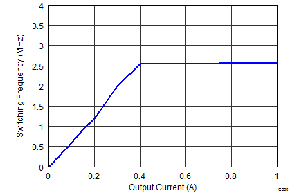
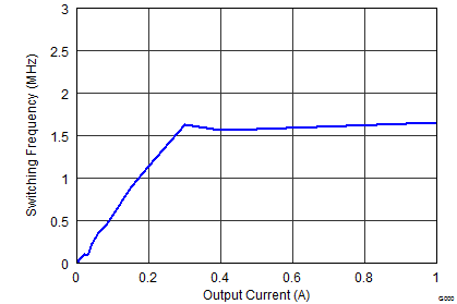
Figure 25. Switching Frequency vs Output Current
TPS62150A-Q1 TPS62152A-Q1 TPS62153A-Q1 SLVSAL5_fswiout_3.3V.png
FSW = Low VOUT = 3.3 V
Figure 27. Switching Frequency vs Output Current
TPS62150A-Q1 TPS62152A-Q1 TPS62153A-Q1 SLVSAL5_fswiout_1.8V.png
FSW = Low VOUT = 1.8 V
Figure 29. Switching Frequency vs Output Current
TPS62150A-Q1 TPS62152A-Q1 TPS62153A-Q1 SLVSAL5_fswiout_1.0V.png
FSW = Low VOUT = 1 V
Figure 31. Switching Frequency vs Output Current
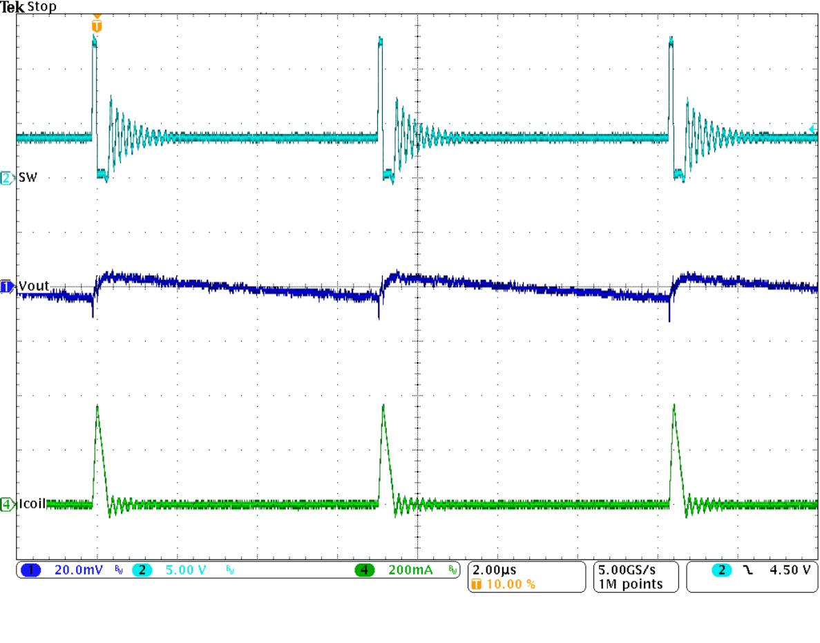
TPS62150A-Q1 TPS62152A-Q1 TPS62153A-Q1 SLVSCC3_PSMtyp.gifFigure 33. Typical Operation in Power Save Mode (IOUT = 10mA)
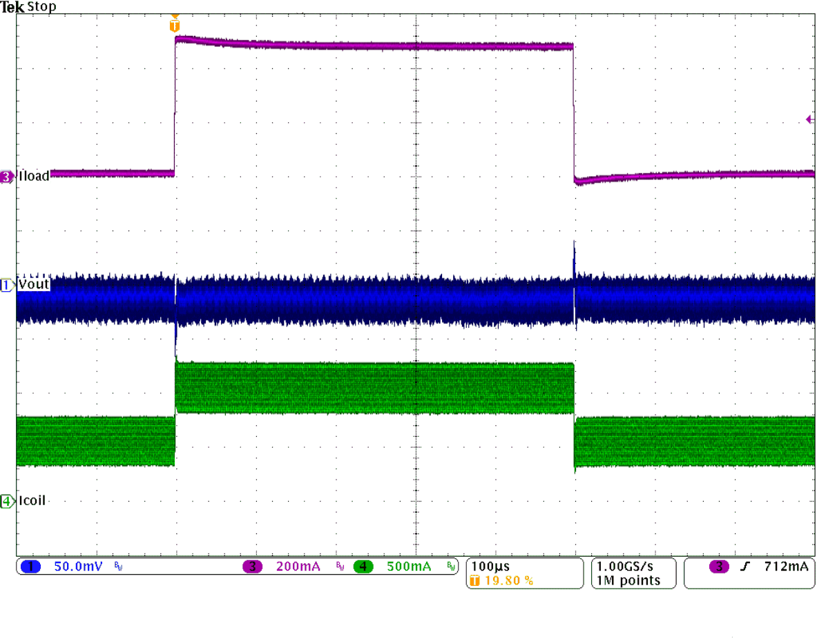
TPS62150A-Q1 TPS62152A-Q1 TPS62153A-Q1 SLVSCC3_loadtranfull.gifFigure 35. Load Transient Response (0.5 to 1 to 0.5 A)
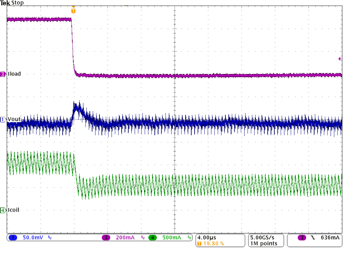
TPS62150A-Q1 TPS62152A-Q1 TPS62153A-Q1 SLVSCC3_loadtranfall.gifFigure 37. Load Transient Response of Figure 35,
Falling Edge
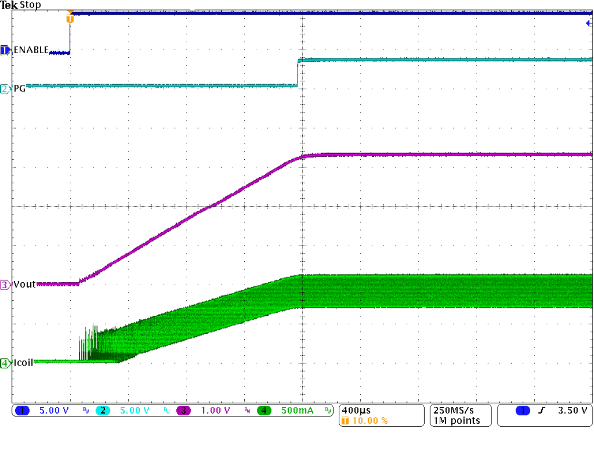
TPS62150A-Q1 TPS62152A-Q1 TPS62153A-Q1 SLVSCC3_stuphigh.gifFigure 39. Start Up Into 1A