ZHCSCG9C May 2014 – July 2019 TPS62150A-Q1 , TPS62152A-Q1 , TPS62153A-Q1
PRODUCTION DATA.
- 1 特性
- 2 应用
- 3 说明
- 4 修订历史记录
- 5 Device Comparison Table
- 6 Pin Configuration and Functions
- 7 Specifications
- 8 Parameter Measurement Information
-
9 Detailed Description
- 9.1 Overview
- 9.2 Functional Block Diagram
- 9.3
Feature Description
- 9.3.1 Pulse Width Modulation (PWM) Operation
- 9.3.2 Power Save Mode Operation
- 9.3.3 100% Duty-Cycle Operation
- 9.3.4 Enable / Shutdown (EN)
- 9.3.5 Soft Start / Tracking (SS/TR)
- 9.3.6 Current Limit And Short Circuit Protection
- 9.3.7 Power Good (PG)
- 9.3.8 Pin-Selectable Output Voltage (DEF)
- 9.3.9 Frequency Selection (FSW)
- 9.3.10 Under Voltage Lockout (UVLO)
- 9.3.11 Thermal Shutdown
- 9.4 Device Functional Modes
-
10Application and Implementation
- 10.1 Application Information
- 10.2
Typical Application
- 10.2.1
TPS62150A-Q1 Point-Of-Load Step Down Converter
- 10.2.1.1 Design Requirements
- 10.2.1.2
Detailed Design Procedure
- 10.2.1.2.1 Custom Design With WEBENCH® Tools
- 10.2.1.2.2 Programming The Output Voltage
- 10.2.1.2.3 External Component Selection
- 10.2.1.2.4 Inductor Selection
- 10.2.1.2.5 Output Capacitor
- 10.2.1.2.6 Input Capacitor
- 10.2.1.2.7 Soft Start Capacitor
- 10.2.1.2.8 Tracking Function
- 10.2.1.2.9 Output Filter And Loop Stability
- 10.2.1.3 Application Curves
- 10.2.2 System Examples
- 10.2.1
TPS62150A-Q1 Point-Of-Load Step Down Converter
- 11Power Supply Recommendations
- 12Layout
- 13器件和文档支持
- 14机械、封装和可订购信息
10.2.2.2 Inverting Power Supply
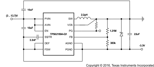
The TPS62150A-Q1 can be used as inverting power supply by rearranging external circuitry as shown in Figure 41.
spacing
 Figure 41. –3.3 V Inverting Power Supply
 spacing
As the former GND node now represents a voltage level below system ground, the voltage difference between VIN and VOUT has to be limited for operation to the maximum supply voltage of 17V (see Equation 16).
spacing

spacing
The transfer function of the inverting power supply configuration differs from the buck mode transfer function, incorporating a Right Half Plane Zero additionally. The loop stability has to be adapted and an output capacitance of at least 22µF is recommended. A detailed design example is given in SLVA469.