ZHCSCG9C May 2014 – July 2019 TPS62150A-Q1 , TPS62152A-Q1 , TPS62153A-Q1
PRODUCTION DATA.
- 1 特性
- 2 应用
- 3 说明
- 4 修订历史记录
- 5 Device Comparison Table
- 6 Pin Configuration and Functions
- 7 Specifications
- 8 Parameter Measurement Information
-
9 Detailed Description
- 9.1 Overview
- 9.2 Functional Block Diagram
- 9.3
Feature Description
- 9.3.1 Pulse Width Modulation (PWM) Operation
- 9.3.2 Power Save Mode Operation
- 9.3.3 100% Duty-Cycle Operation
- 9.3.4 Enable / Shutdown (EN)
- 9.3.5 Soft Start / Tracking (SS/TR)
- 9.3.6 Current Limit And Short Circuit Protection
- 9.3.7 Power Good (PG)
- 9.3.8 Pin-Selectable Output Voltage (DEF)
- 9.3.9 Frequency Selection (FSW)
- 9.3.10 Under Voltage Lockout (UVLO)
- 9.3.11 Thermal Shutdown
- 9.4 Device Functional Modes
-
10Application and Implementation
- 10.1 Application Information
- 10.2
Typical Application
- 10.2.1
TPS62150A-Q1 Point-Of-Load Step Down Converter
- 10.2.1.1 Design Requirements
- 10.2.1.2
Detailed Design Procedure
- 10.2.1.2.1 Custom Design With WEBENCH® Tools
- 10.2.1.2.2 Programming The Output Voltage
- 10.2.1.2.3 External Component Selection
- 10.2.1.2.4 Inductor Selection
- 10.2.1.2.5 Output Capacitor
- 10.2.1.2.6 Input Capacitor
- 10.2.1.2.7 Soft Start Capacitor
- 10.2.1.2.8 Tracking Function
- 10.2.1.2.9 Output Filter And Loop Stability
- 10.2.1.3 Application Curves
- 10.2.2 System Examples
- 10.2.1
TPS62150A-Q1 Point-Of-Load Step Down Converter
- 11Power Supply Recommendations
- 12Layout
- 13器件和文档支持
- 14机械、封装和可订购信息
10.2.2.4 Various Output Voltages
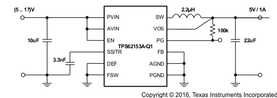
The TPS62150A-Q1 can be set for different output voltages between 0.9V and 6V. Some examples are shown below.
spacing
 Figure 43. 5-V Power Supply Using TPS62153A-Q1 Fixed VOUT Version
 spacing
 Figure 44. 3.3V/1A Power Supply
 spacing
 Figure 45. 2.5V/1A Power Supply
 spacing
 Figure 46. 1.8V/1A Power Supply
 spacing
 Figure 47. 1.5V/1A Power Supply
 spacing
 Figure 48. 1.2V/1A Power Supply
 spacing
 Figure 49. 1V/1A Power Supply
 spacing