ZHCSB86E November 2011 – October 2021 TPS62150 , TPS62150A , TPS62151 , TPS62152 , TPS62153
PRODUCTION DATA
- 1 特性
- 2 应用
- 3 说明
- 4 Revision History
- 5 Device Comparison Table
- 6 Pin Configuration and Functions
- 7 Specifications
- 8 Detailed Description
- 9 Application and Implementation
- 10Power Supply Recommendations
- 11Layout
- 12Device and Documentation Support
- 13Mechanical, Packaging, and Orderable Information
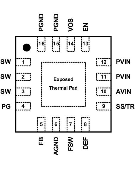
6 Pin Configuration and Functions
 Figure 6-1 16-Pin VQFN
With Thermal PadRGT Package(Top View)
Figure 6-1 16-Pin VQFN
With Thermal PadRGT Package(Top View)Table 6-1 Pin Functions
| PIN(1) | I/O | DESCRIPTION | |
|---|---|---|---|
| NO. | NAME | ||
| 1,2,3 | SW | O | Switch node, which is connected to the internal MOSFET switches. Connect the inductor between SW and output capacitor. |
| 4 | PG | O | Output power good (high = VOUT ready, low = VOUT below nominal regulation); open drain (requires pullup resistor) |
| 5 | FB | I | Voltage feedback of the adjustable version. Connect a resistive voltage divider to this pin. It is recommended to connect FB to AGND on fixed output voltage versions for improved thermal performance. |
| 6 | AGND | Analog Ground. Must be connected directly to the exposed thermal pad and common ground plane. | |
| 7 | FSW | I | Switching Frequency Select (low is approximately 2.5 MHz, high is approximately 1.25 MHz(2) for typical operation)(3) |
| 8 | DEF | I | Output Voltage Scaling (low = nominal, high = nominal + 5%)(3) |
| 9 | SS/TR | I | Soft-Start / Tracking Pin. An external capacitor connected to this pin sets the internal voltage reference rise time. It can be used for tracking and sequencing. |
| 10 | AVIN | I | Supply voltage for control circuitry. Connect to same source as PVIN. |
| 11,12 | PVIN | I | Supply voltage for power stage. Connect to same source as AVIN. |
| 13 | EN | I | Enable input (high = enabled, low = disabled)(3) |
| 14 | VOS | I | Output voltage sense pin and connection for the control loop circuitry |
| 15,16 | PGND | Power Ground. Must be connected directly to the exposed thermal pad and common ground plane. | |
| Exposed Thermal Pad | Must be connected to AGND (pin 6), PGND (pin 15,16), and common ground plane. See the Layout Example. Must be soldered to achieve appropriate power dissipation and mechanical reliability. | ||
(2) Connect FSW to VOUT or PG in this case.
(3) An internal pulldown resistor keeps logic level low, if pin is
floating.