ZHCS504E November 2011 – May 2017 TPS62160 , TPS62161 , TPS62162 , TPS62163
PRODUCTION DATA.
- 1 特性
- 2 应用
- 3 说明
- 4 修订历史记录
- 5 Device Voltage Options
- 6 Pin Configuration and Functions
- 7 Specifications
- 8 Detailed Description
- 9 Application and Implementation
- 10Power Supply Recommendations
- 11Layout
- 12器件和文档支持
- 13机械、封装和可订购信息
9 Application and Implementation
NOTE
Information in the following applications sections is not part of the TI component specification, and TI does not warrant its accuracy or completeness. TI’s customers are responsible for determining suitability of components for their purposes. Customers should validate and test their design implementation to confirm system functionality.
9.1 Application Information
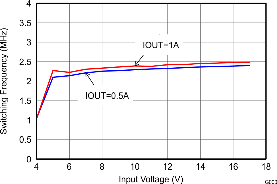
The TPS6216x device family are easy to use synchronous step-down DC/DC converters optimized for applications with high power density. A high switching frequency of typically 2.25 MHz allows the use of small inductors and provides fast transient response as well as high output voltage accuracy by utilization of the DCS-Control™ topology. With its wide operating input voltage range of 3 V to 17 V, the devices are ideally suited for systems powered from either a Li-Ion or other battery as well as from 12-V intermediate power rails. It supports up to 1-A continuous output current at output voltages between 0.9 V and 6 V (with 100% duty cycle mode).
9.2 Typical Application
SPACE
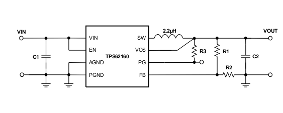 Figure 7. TPS62160 Adjustable Power Supply
space
9.2.1 Design Requirements
The design guideline provides a component selection to operate the device within the Recommended Operating Conditions.
9.2.2 Detailed Design Procedure
9.2.2.1 Custom Design with WEBENCH® Tools
Click here to create a custom design using the TPS62160 device with the WEBENCH® Power Designer.
- Start by entering your VIN, VOUT, and IOUT requirements.
- Optimize your design for key parameters like efficiency, footprint and cost using the optimizer dial and compare this design with other possible solutions from Texas Instruments.
- The WEBENCH Power Designer provides you with a customized schematic along with a list of materials with real time pricing and component availability.
- In most cases, you will also be able to:
- Run electrical simulations to see important waveforms and circuit performance
- Run thermal simulations to understand the thermal performance of your board
- Export your customized schematic and layout into popular CAD formats
- Print PDF reports for the design, and share your design with colleagues
- Get more information about WEBENCH tools at www.ti.com/WEBENCH.
9.2.2.2 Programming the Output Voltage
While the output voltage of the TPS62160 is adjustable, the TPS62161/TPS62162/TPS62163 are programmed to fixed output voltages. For fixed output versions, the FB pin is pulled down internally and may be left floating. It is recommended to connect it to AGND to improve thermal resistance. The adjustable version can be programmed for output voltages from 0.9 V to 6 V by using a resistive divider from VOUT to AGND. The voltage at the FB pin is regulated to 800 mV. The value of the output voltage is set by the selection of the resistive divider from Equation 6. It is recommended to choose resistor values which allow a current of at least 2 µA, meaning the value of R2 should not exceed 400 kΩ. Lower resistor values are recommended for highest accuracy and most robust design. For applications requiring lowest current consumption, the use of fixed output voltage versions is recommended.
spacing

spacing
If the FB pin becomes open, the device clamps the output voltage at the VOS pin to about 7.4 V.
9.2.2.3 External Component Selection
The external components have to fulfill the needs of the application, but also the stability criteria of the devices control loop. The TPS6216x is optimized to work within a range of external components. The LC output filter's inductance and capacitance have to be considered together, creating a double pole, responsible for the corner frequency of the converter (see Output Filter and Loop Stability section). Table 2 can be used to simplify the output filter component selection. Checked cells represent combinations that are proven for stability by simulation and lab test. Further combinations should be checked for each individual application.
space
Table 2. Recommended LC Output Filter Combinations(1)
| 4.7µF | 10µF | 22µF | 47µF | 100µF | 200µF | 400µF | |
|---|---|---|---|---|---|---|---|
| 1µH | |||||||
| 2.2µH | √ | √(2) | √ | √ | √ | ||
| 3.3µH | √ | √ | √ | √ | |||
| 4.7µH |
space
More detailed information on further LC combinations can be found in SLVA463.
9.2.2.4 Inductor Selection
The inductor selection is affected by several effects like inductor ripple current, output ripple voltage, PWM-to-PSM transition point and efficiency. In addition, the inductor selected has to be rated for appropriate saturation current and DC resistance (DCR). Equation 7 and Equation 8 calculate the maximum inductor current under static load conditions.
spacing

spacing
spacing
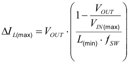
where
- IL(max) is the maximum inductor current
- ΔIL is the peak-to-peak inductor ripple current
- L(min) is the minimum effective inductor value
- fSW is the actual PWM switching frequency
spacing
Calculating the maximum inductor current using the actual operating conditions gives the minimum saturation current of the inductor needed. A margin of about 20% is recommended to add. A larger inductor value is also useful to get lower ripple current, but increases the transient response time and size as well. The following inductors have been used with the TPS6216x and are recommended for use:
Table 3. List of Inductors(1)
| Type | Inductance [µH] | Current [A](2) | Dimensions [L x B x H] mm | Manufacturer |
|---|---|---|---|---|
| VLF3012ST-2R2M1R4 | 2.2 µH, ±20% | 1.9 A | 3.0 x 2.8 x 1.2 | TDK |
| VLF302512MT-2R2M | 2.2 µH, ±20% | 1.9 A | 3.0 x 2.5 x 1.2 | TDK |
| VLS252012T-2R2M1R3 | 2.2 uH, ±20% | 1.3 A | 2.5 x 2.0 x 1.2 | TDK |
| XFL3012-222MEC | 2.2 µH, ±20% | 1.9 A | 3.0 x 3.0 x 1.2 | Coilcraft |
| XFL3012-332MEC | 3.3 µH, ±20% | 1.6 A | 3.0 x 3.0 x 1.2 | Coilcraft |
| LPS3015-332ML_ | 3.3 uH, ±20% | 1.4 A | 3.0 x 3.0 x 1.4 | Coilcraft |
| NR3015T-2R2M | 2.2 uH, ±20% | 1.5 A | 3.0 x 3.0 x 1.5 | Taiyo Yuden |
| 744025003 | 3.3 uH, ±20% | 1.5 A | 2.8 x 2.8 x 2.8 | Wuerth |
| PSI25201B-2R2MS | 2.2 uH, ±20% | 1.3 A | 2.0 x 2.5 x 1.2 | Cyntec |
The TPS6216x can operate with an inductor as low as 2.2 µH. However, for applications with low input voltages, 3.3 µH is recommended to allow the full output current. The inductor value also determines the load current at which Power Save Mode is entered:
spacing

spacing
Using Equation 8, this current level is adjusted by changing the inductor value.
9.2.2.5 Capacitor Selection
9.2.2.5.1 Output Capacitor
The recommended value for the output capacitor is 22 uF. The architecture of the TPS6216x allows the use of tiny ceramic output capacitors with low equivalent series resistance (ESR). These capacitors provide low output voltage ripple and are recommended. To keep its low resistance up to high frequencies and to get narrow capacitance variation with temperature, it is recommended to use an X7R or X5R dielectric. Using a higher value can have some advantages like smaller voltage ripple and a tighter DC output accuracy in power save mode (see SLVA463).
Note: In power save mode, the output voltage ripple depends on the output capacitance, its ESR and the peak inductor current. Using ceramic capacitors provides small ESR and low ripple.
9.2.2.5.2 Input Capacitor
For most applications, 10 µF is sufficient and is recommended, though a larger value reduces input current ripple further. The input capacitor buffers the input voltage for transient events and also decouples the converter from the supply. A low ESR multilayer ceramic capacitor is recommended for best filtering and should be placed between VIN and PGND as close as possible to those pins.
spacing
NOTE
DC bias effect: High capacitance ceramic capacitors have a DC bias effect, which has a strong influence on the final effective capacitance. Therefore the right capacitor value has to be chosen carefully. Package size and voltage rating in combination with dielectric material are responsible for differences between the rated capacitor value and the effective capacitance.
spacing
9.2.2.6 Output Filter and Loop Stability
The devices of the TPS6216x family are internally compensated to be stable with L-C filter combinations corresponding to a corner frequency calculated with Equation 10:
spacing

spacing
Proven nominal values for inductance and ceramic capacitance are given in Table 2 and are recommended for use. Different values may work, but care has to be taken on the loop stability which is affected. More information including a detailed L-C stability matrix is found in SLVA463.
The TPS6216X devices, both fixed and adjustable versions, include an internal 25 pF feed forward capacitor, connected between the VOS and FB pins. This capacitor impacts the frequency behavior and sets a pole and zero in the control loop with the resistors of the feedback divider, per Equation 11 and Equation 12:
spacing

spacing
spacing

spacing
Though the TPS6216x devices are stable without the pole and zero being in a particular location, adjusting their location to the specific needs of the application can provide better performance in power save mode and/or improved transient response. An external feed-forward capacitor can also be added. A more detailed discussion on the optimization for stability versus transient response can be found in SLVA289 and SLVA466.
If using ceramic capacitors, the DC bias effect has to be considered. The DC bias effect results in a drop in effective capacitance as the voltage across the capacitor increases (see NOTE in Input Capacitor section).
9.2.2.7 TPS6216x Components List
Table 4 shows the list of components for the Application Curves.
Table 4. List of Components
9.2.3 Application Curves
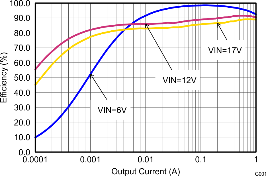
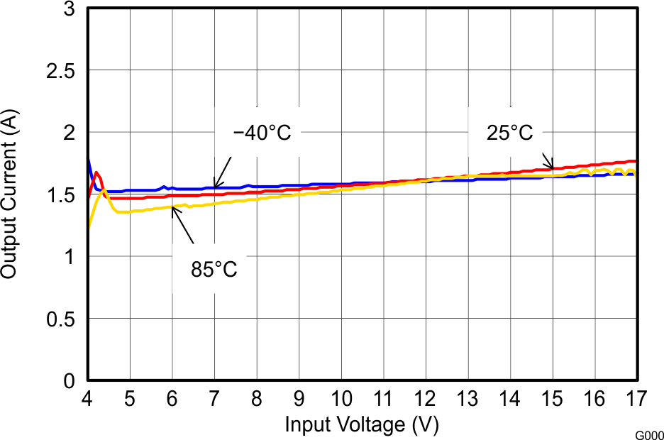
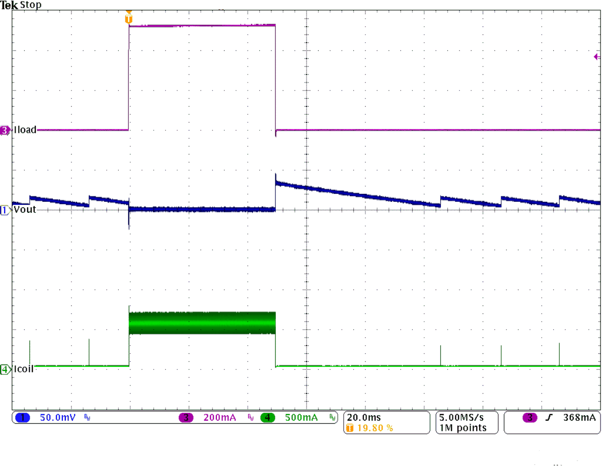
VIN=12 V, VOUT=3.3 V, TA=25°C, (unless otherwise noted)
| VOUT = 6 V | ||
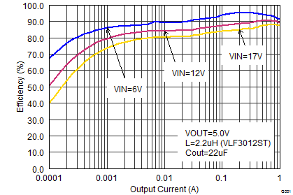
| VOUT = 5 V | ||
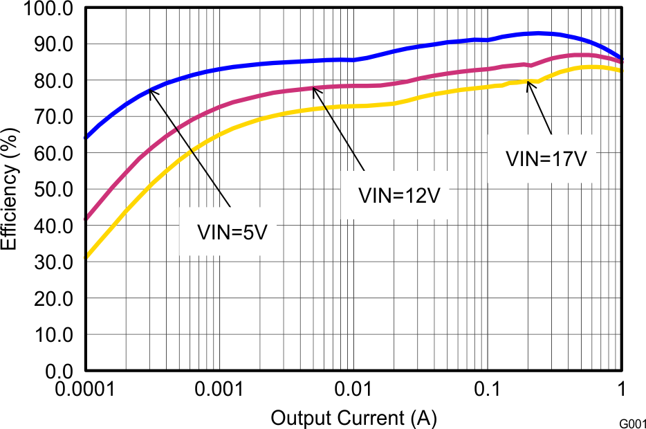
| VOUT = 3.3 V | ||
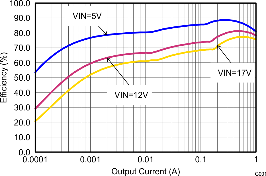
| VOUT = 1.8 V | ||
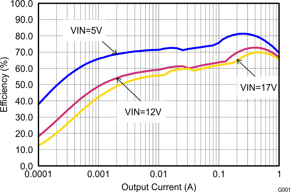
| VOUT = 0.9 V | ||
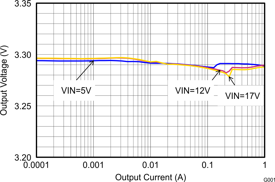
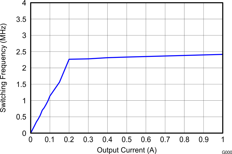
| VIN = 12 V | ||


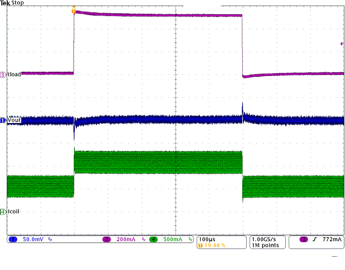
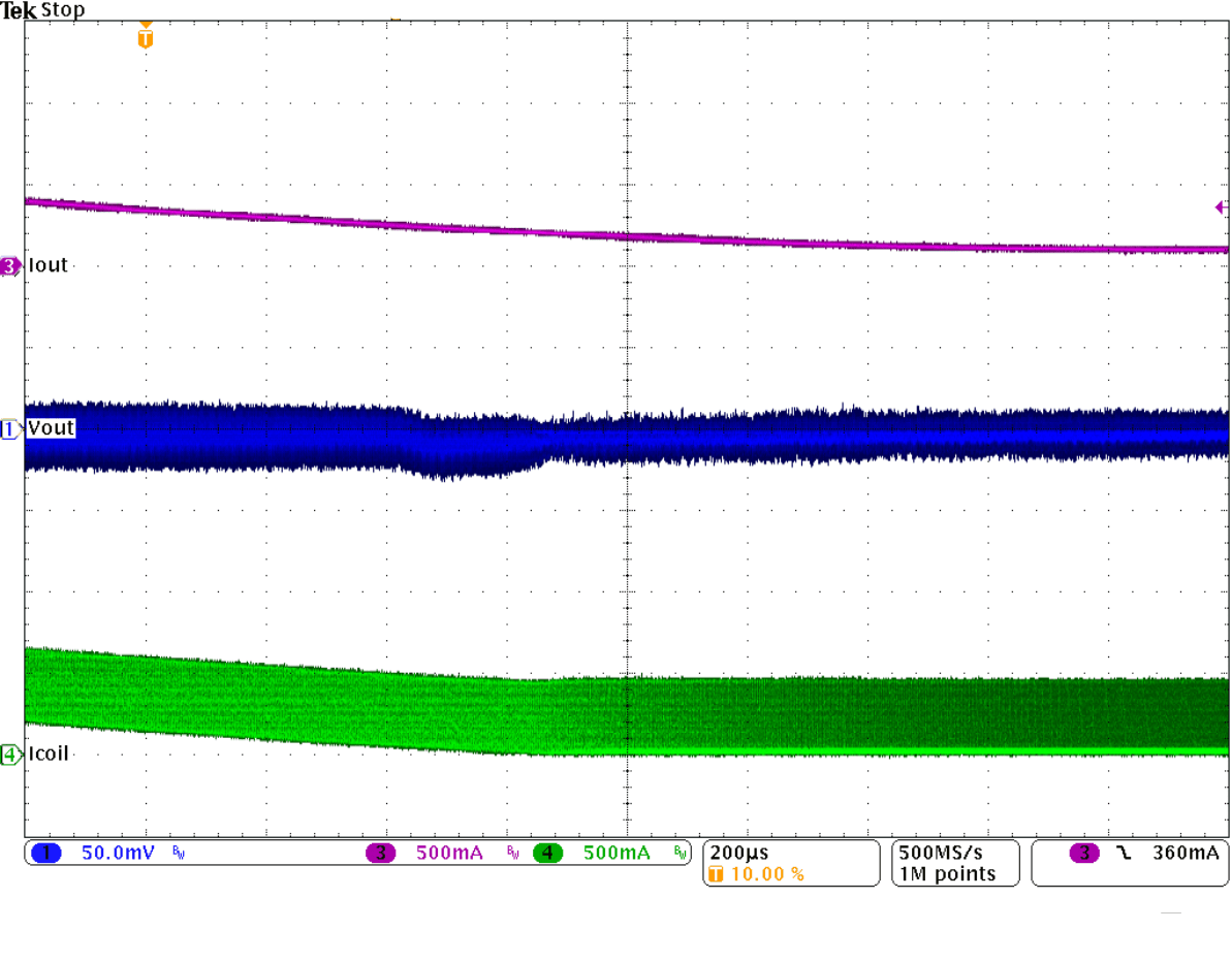
(500 mA to 1 A)
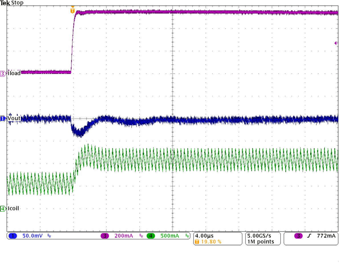
(500 mA to 1 A), Rising Edge
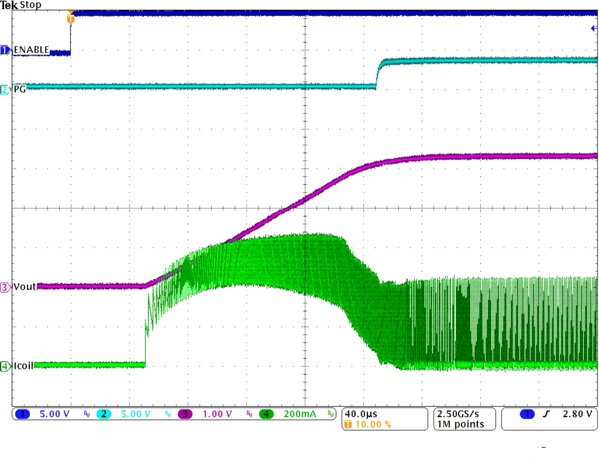
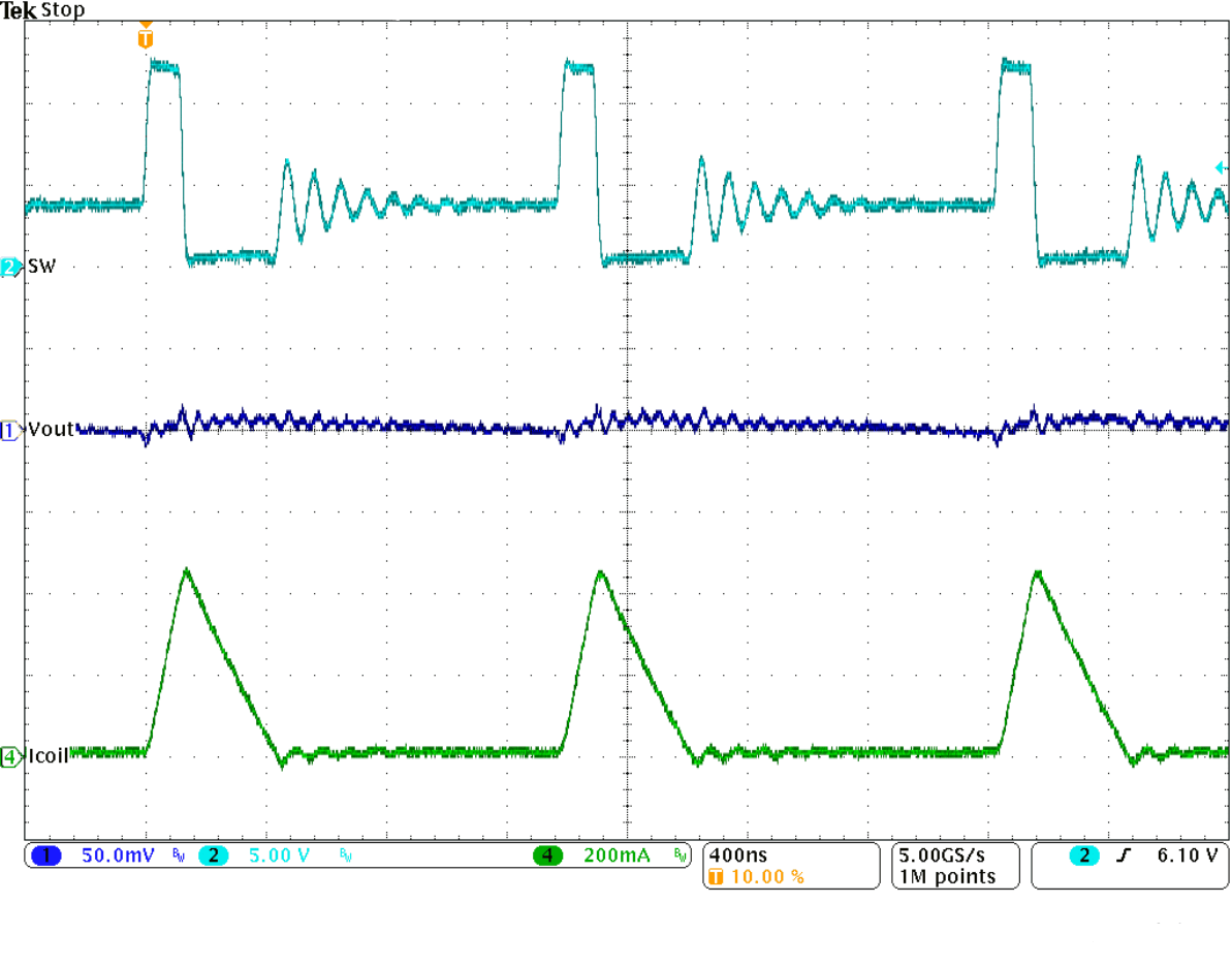
| IOUT = 66 mA | ||
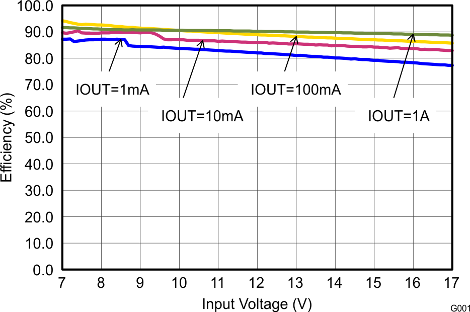
| VOUT = 6 V | ||
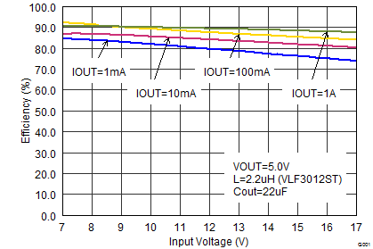
| VOUT = 5 V | ||
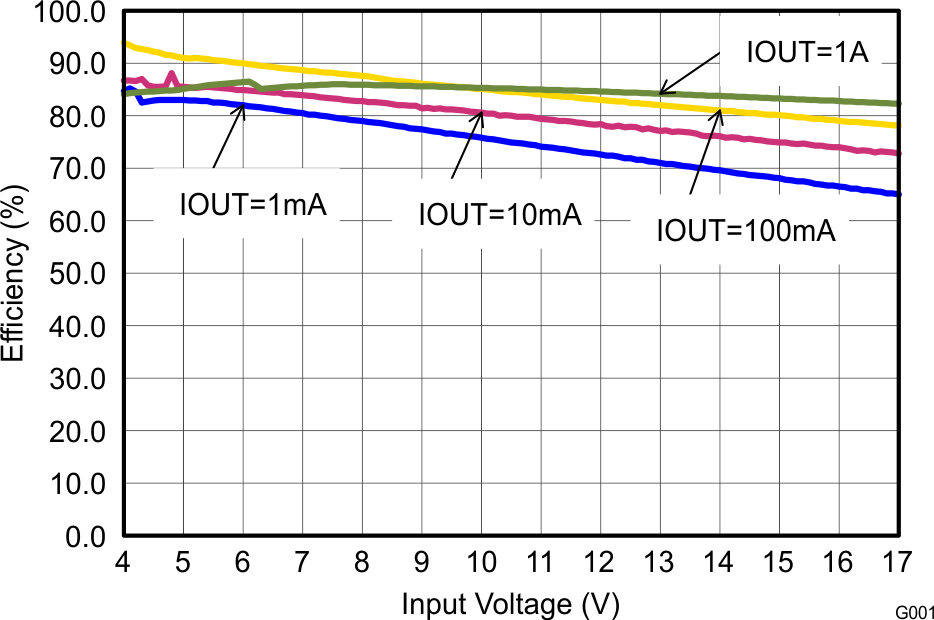
| VOUT = 3.3 V | ||
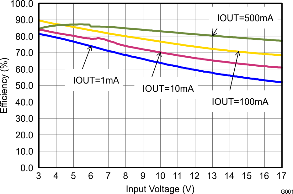
| VOUT = 1.8 V | ||
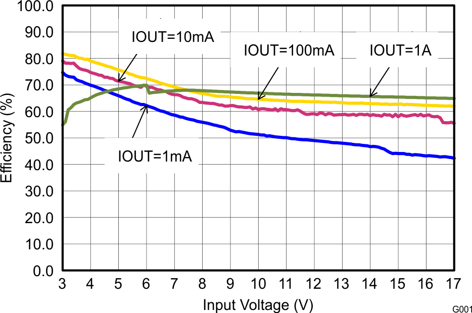
| VOUT = 0.9 V | ||
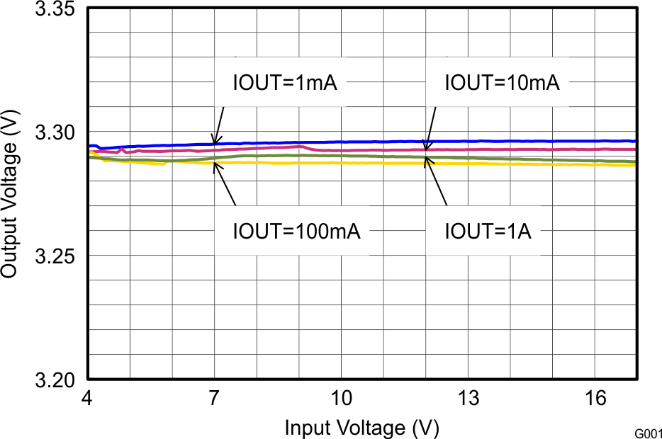
| VOUT = 3.3 V | ||
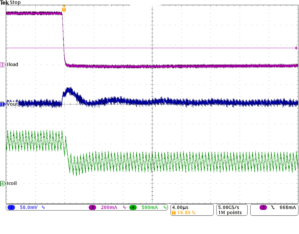
(500 mA to 1 A), Falling Edge
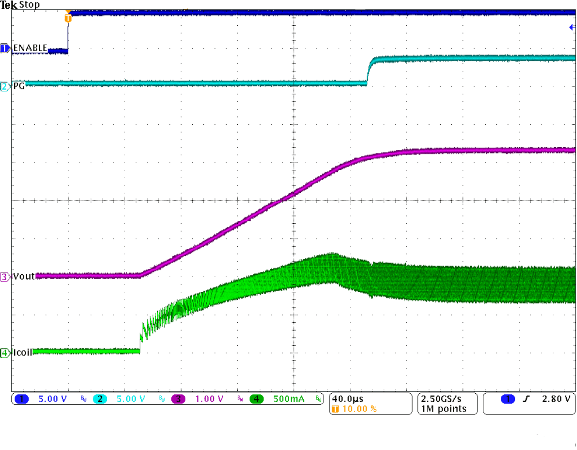
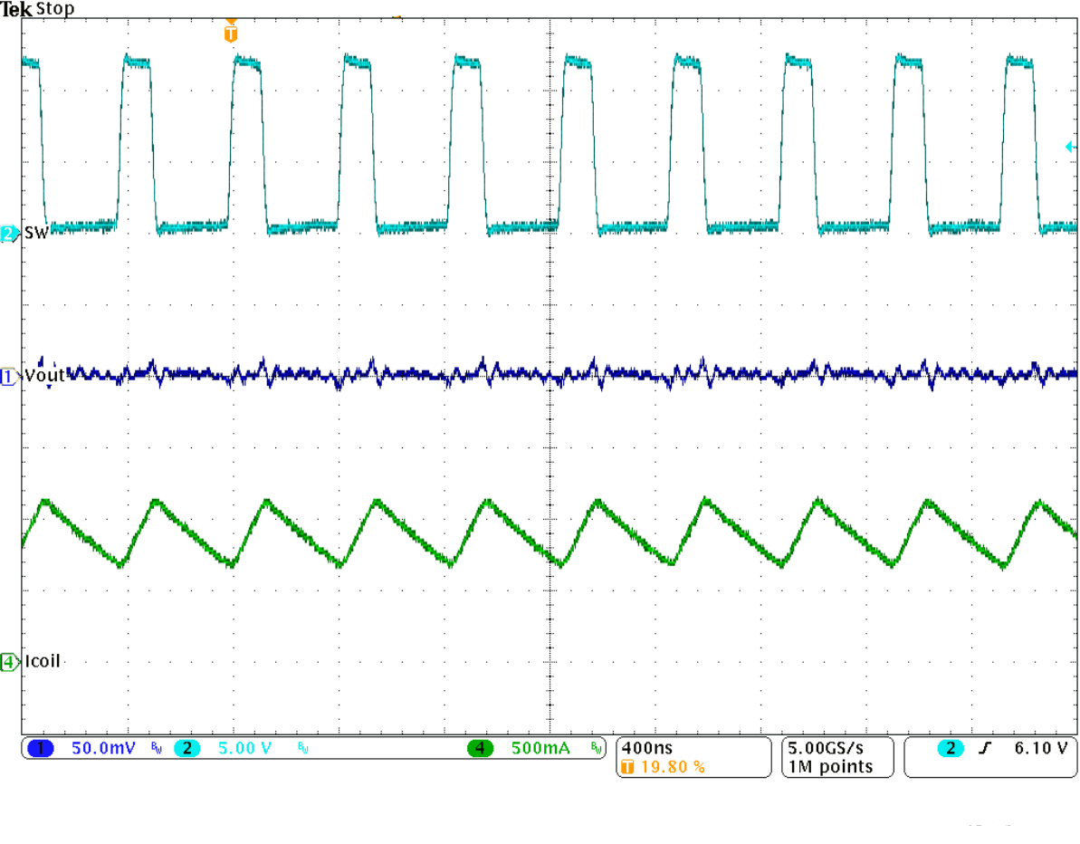
| IOUT = 1 A | ||
9.3 System Examples
9.3.1 1-A Power Supply
The following example circuits show various TPS6216x devices and input voltages that provide a 1-A power supply with output voltage options.
space
space
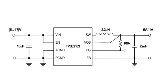 Figure 34. 5 V / 1 A Power Supply
space
space
 Figure 35. 3.3 V / 1 A Power Supply
space
space
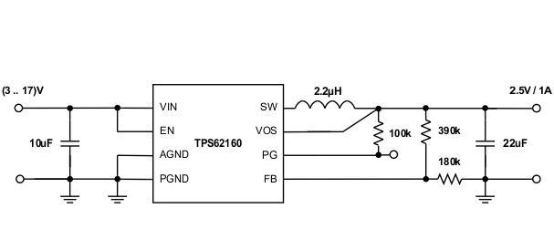 Figure 36. 2.5 V / 1 A Power Supply
space
space
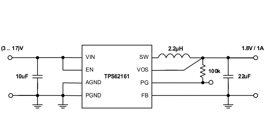 Figure 37. 1.8 V / 1 A Power Supply
space
space
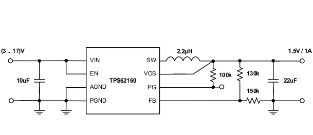 Figure 38. 1.5 V / 1 A Power Supply
space
space
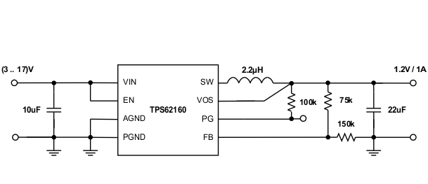 Figure 39. 1.2 V / 1 A Power Supply
space
space
 Figure 40. 1 V / 1 A Power Supply
9.3.2 Inverting Power Supply
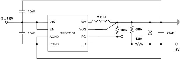
The TPS6216x can be used as inverting power supply by rearranging external circuitry as shown in Figure 41. As the former GND node now represents a voltage level below system ground, the voltage difference between VIN and VOUT has to be limited for operation to the maximum supply voltage of 17 V (see Equation 13).
space
space
space
The transfer function of the inverting power supply configuration differs from the buck mode transfer function, incorporating a right half plane zero additionally. The loop stability has to be adapted and an output capacitance of at least 22 µF is recommended. A detailed design example is given in SLVA469.
space

