ZHCSCQ4B August 2014 – May 2017 TPS62180 , TPS62182
PRODUCTION DATA.
- 1 特性
- 2 应用
- 3 说明
- 4 修订历史记录
- 5 Device Comparison Table
- 6 Pin Configuration and Functions
- 7 Specifications
-
8 Detailed Description
- 8.1 Overview
- 8.2 Functional Block Diagram
- 8.3 Feature Description
- 8.4
Device Functional Modes
- 8.4.1 Pulse Width Modulation (PWM) Operation
- 8.4.2 Power Save Mode (PSM) Operation
- 8.4.3 Minimum Duty Cycle and 100% Mode Operation
- 8.4.4 Automatic Efficiency Enhancement (AEE)
- 8.4.5 Phase-Shifted Operation
- 8.4.6 Current Limit, Current Balancing, and Short Circuit Protection
- 8.4.7 Tracking
- 8.4.8 Operation with Fixed VOUT
- 9 Application and Implementation
- 10Power Supply Recommendations
- 11Layout
- 12器件和文档支持
- 13机械、封装和可订购信息
6 Pin Configuration and Functions
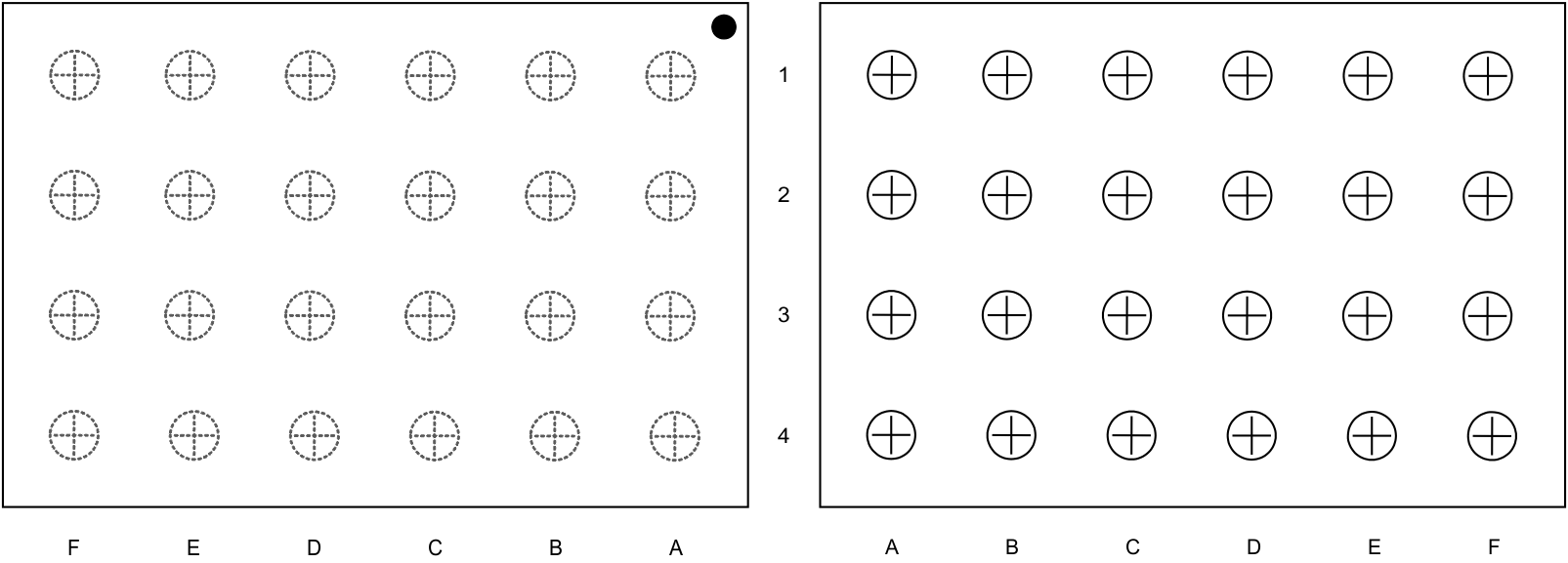
24-Pin DSBGA
YZF Package
(Top View - Left, Bottom View - Right)

Pin Functions
| PIN(1) | DESCRIPTION | |
|---|---|---|
| NAME | NUMBER | |
| AGND | C4 | Analog Ground. Connect on PCB directly with PGND. |
| EN | E4 | Enable input (High = enabled, Low = disabled) |
| FB | B4 | Output voltage feedback. Connect resistive voltage divider to this pin and AGND. On TPS62182, connect to AGND. |
| PG | F4 | Output power good (High = VOUT ready, Low = VOUT below nominal regulation); open drain (requires pull-up resistor) |
| PGND | A3, B3, C3, D3, E3, F3 | Common power ground. |
| SS/TR | D4 | Soft-Start and Tracking Pin. An external capacitor connected to this pin sets the internal voltage reference rise time. |
| SW1 | A2, B2, C2 | Switch node for Phase 1 (master), connected to the internal MOSFET switches. Connect inductor 1 between SW1 and output capacitor. |
| SW2 | D2, E2, F2 | Switch node for Phase 2 (follower), connected to the internal MOSFET switches. Connect inductor 2 between SW2 and output capacitor. |
| VIN1 | A1, B1, C1 | Supply voltage for Phase 1. |
| VIN2 | D1, E1, F1 | Supply voltage for Phase 2. |
| VO | A4 | Output Voltage Connection |
(1) For more information about connecting pins, see Detailed Description and Application Information sections.