ZHCSDE4A December 2014 – February 2015 TPS62184
PRODUCTION DATA.
- 1 特性
- 2 应用
- 3 说明
- 4 简化电路原理图
- 5 修订历史记录
- 6 Pin Configuration and Functions
- 7 Specifications
- 8 Detailed Description
- 9 Application and Implementation
- 10Power Supply Recommendations
- 11Layout
- 12器件和文档支持
- 13机械封装和可订购信息
11 Layout
11.1 Layout Guidelines
The PCB layout of the TPS62184 demands careful attention to ensure proper operation, thermal profile, low noise emission and to achieve best performance. A poor layout can lead to issues like poor regulation, stability and accuracy weaknesses, increased EMI radiation and noise sensitivity. While the TPS62184 provides very high power density, the PCB layout also contributes significantly to the thermal performance.
11.1.1 PCB layout
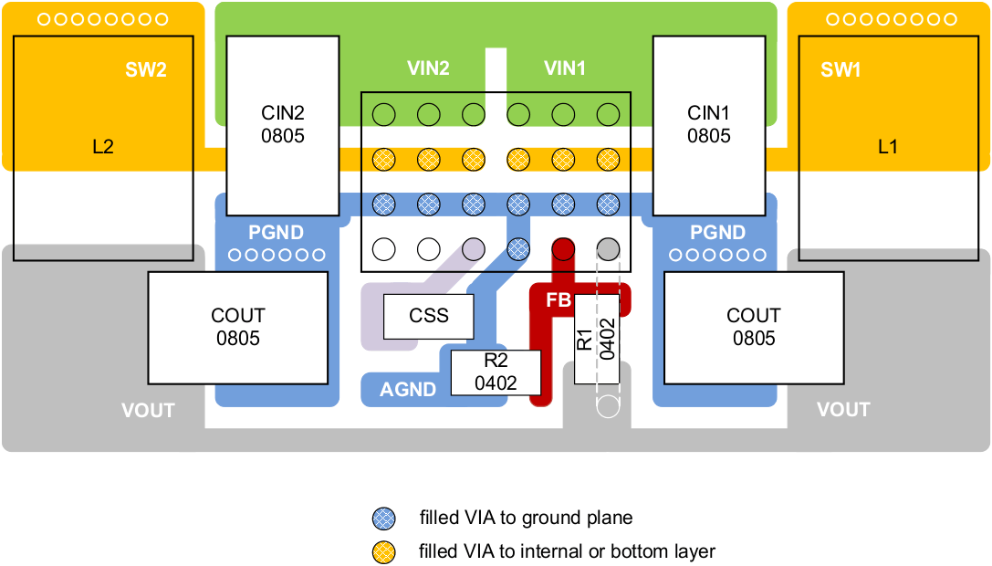
A recommended PCB layout for the TPS62184 dual phase solution is shown below. It ensures best electrical and optimized thermal performance considering the following important topics:
- The input capacitors must be placed as close as possible to the appropriate pins of the device. This provides low resistive and inductive paths for the high di/dt input current. The input capacitance is split, as is the VIN connection, to avoid interference between the input lines.
- The SW node connection from the IC to the inductor conducts high currents. It should be kept short and can be designed in parallel with an internal or bottom layer plane, to provide low resistance and enhanced thermal behavior.
- The VOUT regulation loop is closed with COUT and its ground connection. If a ground layer or plane is used, a direct connection by vias, as shown, is recommended. Otherwise the connection of COUT to GND must be short for good load regulation.
- The FB node is sensitive to dv/dt signals. Therefore the resistive divider should be placed close to the FB pin, avoiding long trace distance.
11.2 Layout Example
 Figure 39. TPS62184 Board Layout