ZHCSDE4A December 2014 – February 2015 TPS62184
PRODUCTION DATA.
- 1 特性
- 2 应用
- 3 说明
- 4 简化电路原理图
- 5 修订历史记录
- 6 Pin Configuration and Functions
- 7 Specifications
- 8 Detailed Description
- 9 Application and Implementation
- 10Power Supply Recommendations
- 11Layout
- 12器件和文档支持
- 13机械封装和可订购信息
8 Detailed Description
8.1 Overview
The TPS62184 is a high efficiency synchronous switched mode step-down converter based on a peak current control topology. It is designed for smallest solution size low-profile applications, converting multi-cell Li-Ion supply voltages to output voltages of 0.9 V to 3.5 V. While an outer voltage loop sets the regulation threshold for the current loop based on the actual VOUT level, the inner current loop adapts the peak inductor current for every switching cycle. The regulation network is internally compensated. The switching frequency is set by an OFF-time control and features Power Save Mode (PSM) and Automatic Efficiency Enhancement (AEE™) to keep the efficiency high over the whole load current and duty cycle range. The switching frequency is set depending on VIN and VOUT and remains unchanged for steady state operating conditions.
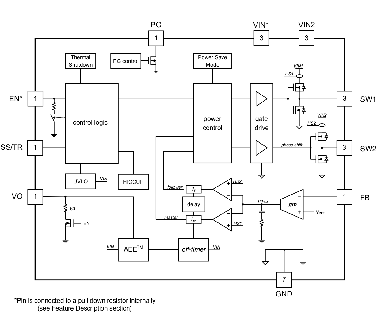
The TPS62184 is a dual phase converter, sharing the load current among the phases. Identical in construction, the follower control loop is connected with a fixed delay to the master control loop. Both the phases use the same regulation threshold and cycle-by-cycle peak current setpoint. This ensures a phase-shifted as well as current-balanced operation. Using the advantages of the dual phase topology, a 6-A continuous output current is provided with high performance and smallest system solution size.
8.2 Functional Block Diagram
 Figure 5. TPS62184
8.3 Feature Description
8.3.1 Enable / Shutdown (EN)
The device starts operation, when VIN is present and Enable (EN) is set High. The EN threshold is 1 V for rising and 0.9 V for falling voltages, providing a threshold accuracy of ±3%. That makes it suitable for precise switching on and off in accurate power sequencing arrangements as well as for slowly rising EN control voltage signals (see Using the Accurate EN Threshold for more details).
The device is disabled by pulling EN Low. A discharge resistor of about 60 Ω is then connected to the output. At the EN pin, an internal pull down resistor of about 350 kΩ keeps the Low state, if EN gets high impedance or floating afterwards.
The EN pin can be connected to VIN to always enable the device. A delay of 1 ms, after VIN exceeds VUVLO, ensures safe operating conditions before the device starts switching. If VIN is already present, a soft start sequence is initiated about 100 µs after EN is pulled High.
8.3.2 Soft Start / Tracking (SS/TR)
The soft start circuit controls the output voltage slope during startup. This avoids excessive inrush current and ensures a controlled output voltage rise time. It also prevents unwanted voltage drop from high impedance power sources or batteries. When EN is set to start device operation, the device starts switching and VOUT rises with a slope, controlled by the external capacitor connected to the SS/TR pin. It is not recommended to leave the SS/TR pin floating, because VOUT may overshoot. Typical startup operation is shown in Application Performance Curves.
The device can track an external voltage (see Tracking). The device can monotonically start into a pre-biased output.
8.3.3 Power Good (PG)
The TPS62184 has a built in power good (PG) function. The PG pin goes High, when the output voltage has reached its nominal value. Otherwise, including when disabled, in UVLO or in thermal shutdown, PG is Low. The PG pin is an open drain output that requires a pull-up resistor and can sink typically 2 mA. If not used, the PG pin can be left floating or grounded.
8.3.4 Undervoltage Lockout (UVLO)
The undervoltage lockout (UVLO) prevents misoperation of the device, if the input voltage drops below the UVLO threshold. It is set to 3.6 V typically with a hysteresis of typically 300mV. (See also Device Functional Modes).
8.3.5 Thermal Shutdown
The junction temperature TJ of the device is monitored by an internal temperature sensor. If TJ exceeds 160°C (typ.), the device goes in thermal shutdown with a hysteresis of typically 20°C. Both the power FETs are turned off, the discharge resistor is connected to the output and the PG pin goes Low. Once TJ has decreased enough, the device resumes normal operation with Soft Start.
8.4 Device Functional Modes
8.4.1 Pulse Width Modulation (PWM) Operation
The TPS62184 is based on a predictive OFF-time peak current control topology, operating with PWM in continuous conduction mode for heavier loads. Since the OFF-time is automatically adjusted according to the actual VIN and VOUT, it provides highest efficiency over the entire input and output voltage range. The OFF-time is calculated as:

While the OFF-time is predicted, the ON-time is set depending on the converter's duty cycle and calculated as:

Thereby the switching frequency is fixed for a given input and output voltage and is calculated as:

Both the master and follower phases regulate to the same level of VOUT with separate current loops, using the same peak current setpoint, cycle by cycle. This provides excellent peak current balancing, independent of inductor dc resistance matching. Since the follower phase operates with a fixed delay to the master phase, also cycle by cycle, phase shifted operation is obtained.
The device features an automatic transition into Power Save Mode, entered at light loads, running in discontinuous conduction mode (DCM).
8.4.2 Power Save Mode (PSM) Operation
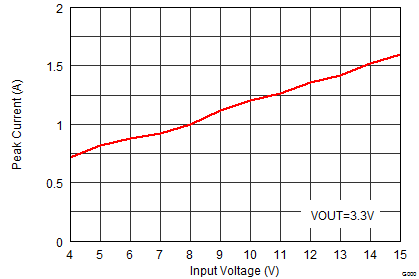
As the load current decreases, the converter enters Power Save Mode operation. During PSM, the converter operates with a reduced switching frequency maintaining highest efficiency due to minimum quiescent current. Power Save Mode is based on a fixed peak current architecture, where the peak current (IPEAK) is set depending on VIN, VOUT, and L. After each single pulse, a pause time until the internal VOUT_Low level threshold is reached completes the switching cycle in PSM.
The switching frequency for PSM in one phase operation is calculated as :

Equation 4 shows the linear relationship of output current and switching frequency. Typical values of the fixed peak current are shown in Figure 6.
 Figure 6. Typical Fixed Peak Current (IPEAK) in Power Save Mode
If the load decreases to very light loads and only one phase is needed, either phase (master or follower) might be active. The load current level at which Power Save Mode is entered is calculated as follows:

Equation 7 is used to calculate ΔIL.
8.4.3 Minimum Duty Cycle and 100% Mode Operation
When the input voltage comes close to the output voltage, the device enters 100% mode and both high-side FETs are continuously switched on as long as VOUT remains below its setpoint. The minimum VIN to maintain output voltage regulation is calculated as:

This allows the conversion of small input to output voltage differences, for example for longest operation time in battery powered applications. In 100% duty cycle mode, the low-side FET is switched off.
While the maximum ON-time is not limited, the AEE feature, explained in the next section, secures a minimum ON-time of about 100 ns.
8.4.4 Automatic Efficiency Enhancement (AEE™)
AEE™ provides highest efficiency over the entire input voltage and output voltage range by automatically adjusting the converter's switching frequency. This is achieved by setting the predictive off-time of the converter.
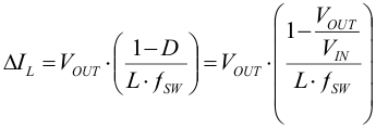
The efficiency of a switched mode converter is determined by the power losses during the conversion. The efficiency decreases, if VOUT decreases and/or VIN increases. In order to keep the efficiency high over the entire duty cycle range (VOUT/VIN ratio), the switching frequency is adjusted while maintaining the ripple current. The following equation shows the relation between the inductor ripple current, switching frequency and duty cycle.

Efficiency increases by decreasing switching losses, preserving high efficiency for varying duty cycles, while the ripple current amplitude remains low enough to deliver the full output current without reaching current limit. The AEE™ feature provides an efficiency enhancement for various duty cycles, especially for lower Vout values, where fixed frequency converters suffer from a significant efficiency drop. Furthermore, this feature compensates for the very small duty cycles of high VIN to low VOUT conversion, which limits the control range in other topologies.
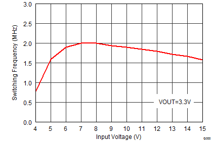
Figure 7 shows the typical switching frequency over the input voltage range.
 Figure 7. Typical Switching Frequency vs Input Voltage
8.4.5 Phase-Shifted Operation
While, for a buck converter, the input current source provides the average current that is needed to support the output current, an input capacitance is needed to support pulse currents. One of the natural benefits of a two- (or multi-) phase converter is the possibility to operate out of phase, which decreases the pulse currents and switching noise. In PWM mode, the TPS62184 runs with a fixed delay of typically 250 ns between the phases. This ensures that the phases run phase-delayed, limiting input RMS current and corresponding noise. If in PSM, both phases run, the phase delay is about 100 ns.
8.4.6 Current Limit, Current Balancing, and Short Circuit Protection
Each phase has a separate integrated peak current limit. While its minimum value limits the output current of the phase, the maximum number gives the current that must be considered to flow in any operating case. If the current limit of a phase is reached, the peak current setpoint is unable to increase further. The device provides its maximum output current. Detecting this heavy load or short circuit condition for about 0.9 ms, the device switches off for about 5 ms and then restarts again with a soft start cycle. As long as the overload condition is present, the device hiccups that way, limiting the output power.
The two phases are peak current balanced with a variation within about ±10% at 6-A output current. Since the control topology does not depend on inductor or output current measurements, the current balancing accuracy is independent of inductor matching (binning) and does not need matched power routing.
8.4.7 Tracking
VOUT can track a voltage that is applied at the SS/TR pin. The tracking range at the SS/TR pin is 50 mV to 1.2 V and the FB pin voltage tracks this as given in Equation 8:

Due to the factor of about 0.64, the minimum output voltage for tracking is 1.25 V. Once the SS/TR pin voltage reaches about 1.2 V, the internal voltage is clamped to the internal feedback voltage and the device goes to normal regulation. This works for falling tracking voltage as well. If, in this case, the SS/TR voltage decreases, the device does not sink current from the output. Thus, the resulting decrease of the output voltage may be slower than the SS/TR pin voltage if the load is light. When driving the SS/TR pin with an external voltage, do not exceed the voltage rating of the SS/TR pin which is VIN+0.3 V.
Note: If the voltage at the FB pin is below its typical value of 0.8 V, the output voltage accuracy may have a wider tolerance than specified.