SLVS417F March 2002 – June 2015 TPS62200 , TPS62201 , TPS62202 , TPS62203 , TPS62204 , TPS62205 , TPS62207 , TPS62208
PRODUCTION DATA.
- 1 Features
- 2 Applications
- 3 Description
- 4 Revision History
- 5 Pin Configuration and Functions
- 6 Specifications
- 7 Detailed Description
- 8 Application and Implementation
- 9 Power Supply Recommendations
- 10Layout
- 11Device and Documentation Support
- 12Mechanical, Packaging, and Orderable Information
7 Detailed Description
7.1 Overview
The TPS6220x device is a synchronous step-down converter operating with typically 1-MHz fixed frequency pulse width modulation (PWM) at moderate to heavy load currents and in power save mode operating with pulse frequency modulation (PFM) at light load currents.
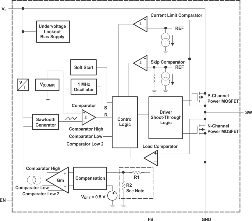
During PWM operation the converter uses a unique fast response, voltage mode, controller scheme with input voltage feed forward. This achieves good line and load regulation and allows the use of small ceramic input and output capacitors. At the beginning of each clock cycle initiated by the clock signal (S), the P-channel MOSFET switch is turned on, and the inductor current ramps up until the comparator trips and the control logic turns off the switch. The current limit comparator also turns off the switch in case the current limit of the P-channel switch is exceeded. Then the N-channel rectifier switch is turned on and the inductor current ramps down. The next cycle is initiated by the clock signal again turning off the N-channel rectifier and turning on the P-channel switch.
The GM amplifier and input voltage determines the rise time of the Sawtooth generator; therefore any change in input voltage or output voltage directly controls the duty cycle of the converter. This gives a very good line and load transient regulation.
7.2 Functional Block Diagram

7.3 Feature Description
7.3.1 Undervoltage Lockout
The undervoltage lockout circuit prevents the device from misoperation at low input voltages. It prevents the converter from turning on the switch or rectifier MOSFET under undefined conditions.
7.3.2 Dynamic Voltage Positioning
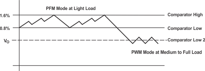
As described in the power save mode operation sections and as detailed in Figure 4, the output voltage is typically 0.8% above the nominal output voltage at light load currents, as the device is in power save mode. This gives additional headroom for the voltage drop during a load transient from light load to full load. During a load transient from full load to light load, the voltage overshoot is also minimized due to active regulation turning on the N-channel rectifier switch.
7.3.3 Soft Start
The TPS6220x has an internal soft start circuit that limits the inrush current during start-up. This prevents possible voltage drops of the input voltage in case a battery or a high-impedance power source is connected to the input of the TPS6220x.
The soft start is implemented as a digital circuit increasing the switch current in steps of typically 60 mA, 120 mA, 240 mA, and then the typical switch current limit of 480 mA. Therefore the start-up time mainly depends on the output capacitor and load current. Typical start-up time with a 10-µF output capacitor and 200-mA load current is 800 µs.
7.3.4 Low Dropout Operation 100% Duty Cycle
The TPS6220x offers a low input to output voltage difference, while still maintaining operation with the 100% duty cycle mode. In this mode, the P-channel switch is constantly turned on. This is particularly useful in battery powered applications to achieve longest operation time by taking full advantage of the whole battery voltage range. The minimum input voltage to maintain regulation, depending on the load current and output voltage, can be calculated as:

where
- Ioutmax = maximum output current plus inductor ripple current.
- rds(ON)max = maximum P-channel switch rds(ON).
- RL = DC resistance of the inductor.
- Voutmax = nominal output voltage plus maximum output voltage tolerance.
7.3.5 Enable
Pulling the enable low forces the part into shutdown, with a shutdown quiescent current of typically 0.1 µA. In this mode, the P-channel switch and N-channel rectifier are turned off, the internal resistor feedback divider is disconnected, and the whole device is in shutdown mode. If an output voltage, which could be an external voltage source or super capacitor, is present during shutdown, the reverse leakage current is specified under Electrical Characteristics. For proper operation the enable pin must be terminated and must not be left floating.
Pulling the enable high starts up the TPS6220x with the soft start as previously described.
7.4 Device Functional Modes
7.4.1 Power Save Mode Operation
As the load current decreases, the converter enters the power save mode operation. During power save mode, the converter operates with reduced switching frequency in PFM mode and with a minimum quiescent current to maintain high efficiency.
Two conditions allow the converter to enter the power save mode operation. One is when the converter detects the discontinuous conduction mode. The other is when the peak switch current in the P-channel switch goes below the skip current limit. The typical skip current limit can be calculated as

During the power save mode, the output voltage is monitored with the comparator by the thresholds comparator low and comparator high. As the output voltage falls below the comparator low threshold set to typically 0.8% above Vout nominal, the P-channel switch turns on. The P-channel switch is turned off as the peak switch current is reached. The typical peak switch current can be calculated:

The N-channel rectifier is turned on and the inductor current ramps down. As the inductor current approaches zero, the N-channel rectifier is turned off and the P-channel switch is turned on again, starting the next pulse. The converter continues these pulses until the comparator high threshold (set to typically 1.6% above Vout nominal) is reached. The converter enters a sleep mode, reducing the quiescent current to a minimum. The converter wakes up again as the output voltage falls below the comparator low threshold again. This control method reduces the quiescent current typically to 15 µA and reduces the switching frequency to a minimum, thereby achieving the high converter efficiency. Setting the skip current thresholds to typically 0.8% and 1.6% above the nominal output voltage at light load current results in a dynamic output voltage achieving lower absolute voltage drops during heavy load transient changes. This allows the converter to operate with a small output capacitor of just 10 µF and still have a low absolute voltage drop during heavy load transient changes. See Figure 4 for detailed operation of the power save mode.
 Figure 4. Power Save Mode Thresholds and Dynamic Voltage Positioning
The converter enters the fixed frequency PWM mode again as soon as the output voltage falls below the comparator low 2 threshold.