ZHCSHS4 March   2018 TPS62243-Q1 , TPS62244-Q1

PRODUCTION DATA.  

  1. 特性
  2. 应用
  3. 说明
    1.     Device Images
      1.      典型应用原理图
      2.      效率与输出电流间的关系
  4. 修订历史记录
  5. Device Comparison Table
  6. Pin Configuration and Functions
    1.     Pin Functions
  7. Specifications
    1. 7.1 Absolute Maximum Ratings
    2. 7.2 ESD Ratings
    3. 7.3 Recommended Operating Conditions
    4. 7.4 Thermal Information
    5. 7.5 Electrical Characteristics
    6. 7.6 Typical Characteristics
  8. Detailed Description
    1. 8.1 Overview
    2. 8.2 Functional Block Diagram
    3. 8.3 Feature Description
      1. 8.3.1 Undervoltage Lockout
      2. 8.3.2 Enable
      3. 8.3.3 Thermal Shutdown
    4. 8.4 Device Functional Modes
      1. 8.4.1 Soft Start
      2. 8.4.2 Power Save Mode
        1. 8.4.2.1 100% Duty Cycle Low Dropout Operation
      3. 8.4.3 Short-Circuit Protection
  9. Application and Implementation
    1. 9.1 Application Information
    2. 9.2 Typical Application
      1. 9.2.1 Design Requirements
      2. 9.2.2 Detailed Design Procedure
        1. 9.2.2.1 Output Filter Design (Inductor and Output Capacitor)
          1. 9.2.2.1.1 Inductor Selection
          2. 9.2.2.1.2 Output Capacitor Selection
          3. 9.2.2.1.3 Input Capacitor Selection
      3. 9.2.3 Application Curves
  10. 10Power Supply Recommendations
  11. 11Layout
    1. 11.1 Layout Guidelines
    2. 11.2 Layout Example
  12. 12器件和文档支持
    1. 12.1 第三方米6体育平台手机版_好二三四免责声明
    2. 12.2 接收文档更新通知
    3. 12.3 社区资源
    4. 12.4 商标
    5. 12.5 静电放电警告
    6. 12.6 Glossary
  13. 13机械、封装和可订购信息
    1. 13.1 Package Option Addendum
      1. 13.1.1 Packaging Information
      2. 13.1.2 Tape and Reel Information

封装选项

机械数据 (封装 | 引脚)
散热焊盘机械数据 (封装 | 引脚)
订购信息

Application Curves

The conditions for below application curves are VIN = 3.0V, VOUT= 1.25V and the components listed in Table 2, unless otherwise noted.
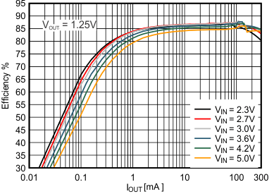
TPS62243-Q1 TPS62244-Q1 SLVSEK3_eff_1p25V.gifFigure 8. Efficiency vs Output Current, VOUT = 1.25V
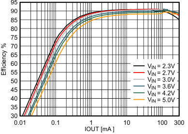
TPS62243-Q1 TPS62244-Q1 SLVSEK3_eff_1p8V.gif
Figure 10. Efficiency vs Output Current, VOUT = 1.8V
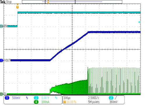
TPS62243-Q1 TPS62244-Q1 Startup_100R_1p25V_3V.gif
VIN = 3V RLoad = 100Ω VOUT = 1.25V
Figure 12. Start-Up Timing
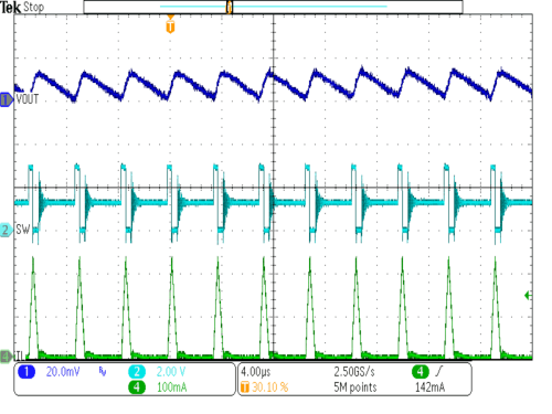
TPS62243-Q1 TPS62244-Q1 SP_3V_1p25V_25mA_PFM.gif
VIN = 3V IOUT = 25mA VOUT = 1.25V
Figure 14. Typical PFM Mode Operation
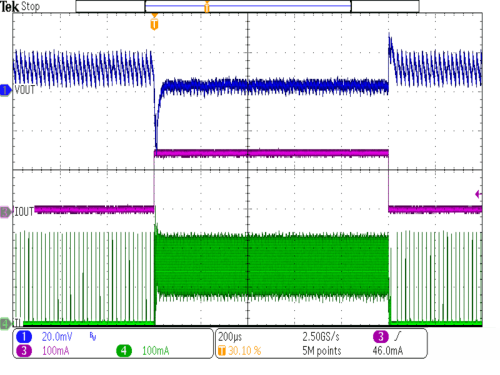
TPS62243-Q1 TPS62244-Q1 loadt_5mA_150mA_3V_1p25V.gif
VIN = 3V IOUT = 5mA to 150mA to 5mA VOUT = 1.25V
Rise / Fall Time 1µs
Figure 16. Load Transient PFM / PWM Mode
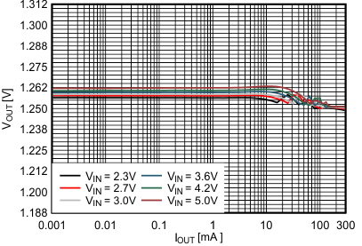
TPS62243-Q1 TPS62244-Q1 SLVSEK3_VO_1p25V_25DC.gifFigure 9. Output Voltage vs Output Current 1.25V VOUT
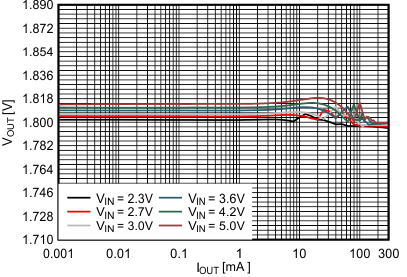
TPS62243-Q1 TPS62244-Q1 SLVSEK3_VO_1p8V25DC.gif
Figure 11. Output Voltage vs Output Current, VOUT = 1.8V
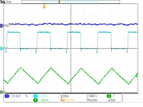
TPS62243-Q1 TPS62244-Q1 SP_3V_1p25V_150mA_PWM.gif
VIN = 3V IOUT = 150mA VOUT = 1.25V
Figure 13. Typical PWM Mode Operation
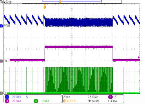
TPS62243-Q1 TPS62244-Q1 loadt_1mA_25mA_3V_1p25V.gif
VIN = 3V IOUT = 1mA to 25mA to 1mA VOUT = 1.25V
Rise / Fall Time 1µs
Figure 15. Load Transient PFM Mode
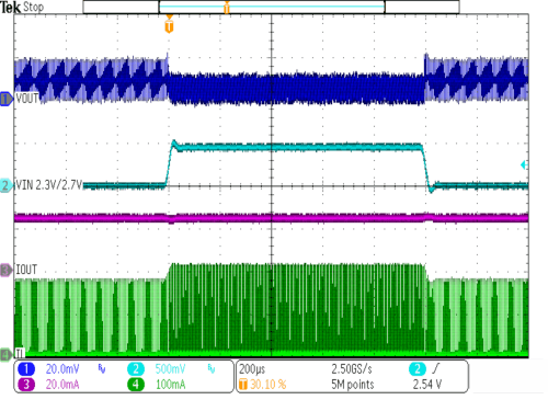
TPS62243-Q1 TPS62244-Q1 linetr_2p3V_2p7V_25mA.gif
VIN = 2.3V to 2.7V to 2.3V IOUT = 25mA VOUT = 1.25V
Rise / Fall Time 10µs
Figure 17. Line Transient PFM Mode