ZHCSI42G June   2007  – April 2018 TPS62290 , TPS62291 , TPS62293

PRODUCTION DATA.  

  1. 特性
  2. 应用
  3. 说明
    1.     Device Images
      1.      典型应用电路原理图
      2.      效率与输出电流间的关系
  4. 修订历史记录
  5. Device Comparison Table
  6. Pin Configuration and Functions
    1.     Pin Functions
  7. Specifications
    1. 7.1 Absolute Maximum Ratings
    2. 7.2 ESD Ratings
    3. 7.3 Recommended Operating Conditions
    4. 7.4 Thermal Information
    5. 7.5 Electrical Characteristics
    6. 7.6 Typical Characteristics
  8. Detailed Description
    1. 8.1 Overview
    2. 8.2 Functional Block Diagram
    3. 8.3 Feature Description
      1. 8.3.1 Dynamic Voltage Positioning
      2. 8.3.2 Enable
      3. 8.3.3 Mode Selection
      4. 8.3.4 Undervoltage Lockout
      5. 8.3.5 Thermal Shutdown
    4. 8.4 Device Functional Modes
      1. 8.4.1 Soft-Start
      2. 8.4.2 Power Save Mode
      3. 8.4.3 100% Duty Cycle Low Dropout Operation
      4. 8.4.4 Short-Circuit Protection
  9. Application and Implementation
    1. 9.1 Application Information
    2. 9.2 Typical Application
      1. 9.2.1 Design Requirements
      2. 9.2.2 Detailed Design Procedure
        1. 9.2.2.1 Output Voltage Setting
        2. 9.2.2.2 Output Filter Design (Inductor and Output Capacitor)
          1. 9.2.2.2.1 Inductor Selection
          2. 9.2.2.2.2 Output Capacitor Selection
          3. 9.2.2.2.3 Input Capacitor Selection
      3. 9.2.3 Application Curves
    3. 9.3 System Examples
  10. 10Power Supply Recommendations
  11. 11Layout
    1. 11.1 Layout Guidelines
    2. 11.2 Layout Example
  12. 12器件和文档支持
    1. 12.1 器件支持
      1. 12.1.1 Third-Party Products Disclaimer
    2. 12.2 相关链接
    3. 12.3 社区资源
    4. 12.4 商标
    5. 12.5 静电放电警告
    6. 12.6 术语表
  13. 13机械、封装和可订购信息

封装选项

机械数据 (封装 | 引脚)
散热焊盘机械数据 (封装 | 引脚)
订购信息

Pin Configuration and Functions

DRV Package
6-PIN SON
Top View
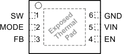
TPS62290 TPS62291 TPS62293 po1_lvs764_ETP.gif

Pin Functions

PIN TYPE DESCRIPTION
NAME NO.
EN 4 IN This is the enable pin of the device. Pulling this pin to low forces the device into shutdown mode. Pulling this pin to high enables the device. This pin must be terminated.
FB 3 IN Feedback pin for the internal regulation loop. Connect the external resistor divider to this pin. In case of fixed output voltage option, connect this pin directly to the output capacitor
GND 6 PWR GND supply pin
MODE 2 IN MODE pin = High forces the device to operate in fixed-frequency PWM mode. Mode pin = Low enables the power save mode with automatic transition from PFM mode to fixed-frequency PWM mode.
SW 1 OUT This is the switch pin and is connected to the internal MOSFET switches. Connect the external inductor between this terminal and the output capacitor.
VIN 5 PWR VIN power supply pin.
Exposed Thermal Pad Connect the exposed thermal pad to GND.