ZHCSEQ2A February 2016 – February 2016 TPS62480
PRODUCTION DATA.
- 1 特性
- 2 应用范围
- 3 说明
- 4 修订历史记录
- 5 Pin Configuration and Functions
- 6 Specifications
- 7 Detailed Description
- 8 Application and Implementation
- 9 Power Supply Recommendations
- 10Layout
- 11器件和文档支持
- 12机械、封装和可订购信息
10 Layout
10.1 Layout Guidelines
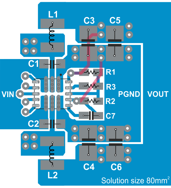
A recommended PCB layout for the TPS62480 dual phase solution is shown below. It ensures best electrical and optimized thermal performance considering the following important topics:
- The input capacitors must be placed as close as possible to the appropriate pins of the device. This provides low resistive and inductive paths for the high di/dt input current. The input capacitance is split, as is the VIN connection, to avoid interference between the input lines.
- The SW node connection from the IC to the inductor conducts high currents. It should be kept short and can be designed in parallel with an internal or bottom layer plane, to provide low resistance and enhanced thermal behavior.
- The VOUT regulation loop is closed with COUT and its ground connection. To avoid PGND noise crosstalk, PGND is kept split for the regulation loop. If a ground layer or plane is used, a direct connection by vias, as shown, is recommended. Otherwise the connection of COUT to GND must be short for good load regulation.
- The use of thermal (filled) vias underneath the device is recommended for improved thermal performance.
- The FB node is sensitive to dv/dt signals. Therefore the resistive divider should be placed close to the FB (and RS pin in case of using R3) pin, avoiding long trace distance.
For more detailed information about the actual 4 layer EVM solution, see SLVUAI6.
10.2 Layout Example
space
 Figure 46. TPS62480 Board Layout