ZHCSEQ2A February 2016 – February 2016 TPS62480
PRODUCTION DATA.
- 1 特性
- 2 应用范围
- 3 说明
- 4 修订历史记录
- 5 Pin Configuration and Functions
- 6 Specifications
- 7 Detailed Description
- 8 Application and Implementation
- 9 Power Supply Recommendations
- 10Layout
- 11器件和文档支持
- 12机械、封装和可订购信息
8 Application and Implementation
space
NOTE
Information in the following applications sections is not part of the TI component specification, and TI does not warrant its accuracy or completeness. TI’s customers are responsible for determining suitability of components for their purposes. Customers should validate and test their design implementation to confirm system functionality.
space
8.1 Application Information
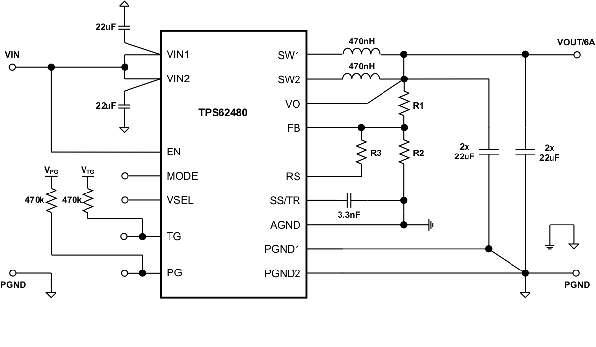
The TPS62480 is a switched mode step-down converter, able to convert a 2.4-V to 5.5-V input voltage into a lower 0.6-V to 5.5-V output voltage, providing up to 6 A continuous output current. It needs a minimum amount of external components. Apart from the LC output filter and the input capacitors, additional resistors or capacitors are only needed to enable features like soft start, adjustable and selectable output voltage as well as Power Good and/or Thermal Good.
8.2 Typical Application
space
space
8.2.1 Design Requirements
The following design guideline provides a range for the component selection to operate within the recommended operating conditions. Table 1 shows the components selection that was used for the measurements shown in the Application Curves.
Table 1. List of Components
8.2.2 Detailed Design Procedure
8.2.2.1 Setting the Adjustable Output Voltage
While the device regulates the FB voltage to 0,6V, the output voltage is specified from 0.6 to 5.5 V. A resistive divider (from VOUT to FB to AGND) sets the actual output voltage of the TPS62480. Equation 4 and Equation 5 are calculating the values of the resistors. First, determining the current through the resistive divider leads to the total resistance (R1 + R2). A minimum divider current of about 5 µA is recommended and can be higher if needed.
space


space
8.2.2.2 Setting VOUT2 Using the VSEL Feature
A VOUT level, different as set with R1 and R2 (see Setting the Adjustable Output Voltage), can be forced by connecting R3 between FB and RS pins and pulling VSEL High. R3 is calculated using Equation 6.
space

where:
V1 is the lower level output voltage and
V2 the higher level output voltage.
space
8.2.2.3 Output Filter Selection
The TPS62480 is internally compensated and optimized to work for a certain range of L-C combinations. The recommended minimum output capacitance is 4 x 22 µF, that can be ceramic capacitors exclusively. A larger value of COUT might be needed for VOUT ≤ 1.8V, to improve transient response performance, as well as for VOUT > 3.3 V to compensate for voltage bias effects of the ceramic capacitors. The other way round, using of an additional feed forward capacitor can help reducing amount of output capacitance that is needed to achieve a certain transient response target (see Output Capacitor Selection).
8.2.2.4 Inductor Selection
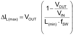
The TPS62480 is designed to operate with two inductors of nominal 470 nH each. Inductors must be selected for adequate saturation current and for low dc resistance (DCR). The minimum inductor current rating IL(min) that is needed under static load conditions calculates using Equation 7 and Equation 8. A current imbalance of 10% is incorporated.
space

space
space
Choosing VIN = 2 VOUT, this calculation provides the minimum saturation current of the inductor needed. Additional margin is recommended to cover dynamic overshoot due to load transients. For low profile solutions, the physical inductor size and the power losses have to be traded off. Smallest solution size gives less efficiency and thermal performance due to larger DCR and/or core losses. The inductors shown in Table 2 have been tested with the TPS62480:
Table 2. List of Inductors
| TYPE | INDUCTANCE [µH] | CURRENT RATING MIN/TYP [A] | DCR MAX [mΩ] | DIMENSIONS (LxBxH) [mm] | MANUFACTURER | |
|---|---|---|---|---|---|---|
| ΔL/L = 30% | ΔT = 40K | |||||
| DFE201612E-R47M | 0.47 ±20% | 5.5/6.1 | 4.5/5.0 | 26 | 2.0 x 1.6 x 1.2 | TOKO |
| DFE252012F-R47M | 0.47 ±20% | 6.7/7.4 | 4.9/5.8 | 22 | 2.5 x 2.0 x 1.2 | TOKO |
| DFE252010F-R47M | 0.47 ±20% | 6.0/6.6 | 4.4/5.2 | 27 | 2.5 x 2.0 x 1.0 | TOKO |
| HMLQ25201B-R47MSR-11 | 0.47 ±20% | 5.6/6.2 | 4.2/4.7 | 28 | 2.5 x 2.0 x 1.2 | CYNTEC |
| HMLQ20161T-R47MDR-11 | 0.47 ±20% | 4.4/4.9 | 4.0/4.4 | 32 | 2.0 x 1.6 x 1.0 | CYNTEC |
| GLCLMR4701A | 0.47 ±20% | 3.6/4.5 | 3.8/4.7 | 32 | 2.5 x 2.0 x 1.2 | ALPS |
| GLCLKR4701A | 0.47 ±20% | 3.5/4.4 | 3.7/4.6 | 38 | 2.5 x 2.0 x 1.0 | ALPS |
| XFL4015-471ME | 0.47 ±20% | 6.6 | 11.2 | 8.36 | 4.0 x 4.0 x 1.5 | COILCRAFT |
space
8.2.2.5 Output Capacitor Selection
The TPS62480 provides a wide output voltage range of 0.6 V to 5.5 V. While stability is a critical criteria for the output filter selection, the output capacitor value also determines transient response behavior, ripple and accuracy of VOUT. The internal compensation is designed for an output capacitance range from about 50 µF to 150 µF effectively. Since ceramic capacitors are used preferably, this translates into nominal values of 4 x 22 µF to 4 x 47 µF and mainly depends on the output voltage. The following values are recommended:
Table 3. Recommended Output Capacitor Values (nominal)
| VOUT ≤ 1.0V | 1.0V ≤ VOUT ≤ 3.3V | VOUT ≥ 3.3V | |||
|---|---|---|---|---|---|
| 2x22µF | |||||
| 4x22µF | √ | ||||
| 4x47µF | √ | √ | √ | ||
| 6x47µF | |||||
space
Beyond the recommendations in Table 3, other values can be chosen and might be suitable depending on VOUT and actual effective capacitance. In such case, stability needs to be checked within the actual environment.
Even if the output capacitance is sufficient for stability, a different value might be desirable to improve the transient response behavior. Table 4 can be used to determine capacitor values for specific transient response targets:
Table 4. Recommended Output Capacitor Values (nominal)
| Output Voltage [V] | Load Step [A] | Output Capacitor Value(1) | Feedforward Capacitor(1) | Typical Transient Response Accuracy | |
|---|---|---|---|---|---|
| ±mV | ±% | ||||
| 1.0 | 0 - 3 | 4 x 47µF | - | 50 | 5 |
| 3 - 6 | 50 | 5 | |||
| 1.8 | 0 - 3 | 4 x 22µF | 36pF | 50 | 3 |
| 3 - 6 | 50 | 3 | |||
| 2.5 | 0 - 3 | 4 x 22µF | 36pF | 62 | 2.5 |
| 3 - 6 | 50 | 2 | |||
| 3.3 | 0 - 3 | 4 x 47µF | 36pF | 100 | 3 |
| 3 - 6 | 80 | 2.5 | |||
space
The architecture of the TPS62480 allows the use of tiny ceramic output capacitors with low equivalent series resistance (ESR). These capacitors provide low output voltage ripple and are recommended. To keep its low resistance up to high frequencies and to get narrow capacitance variation with temperature, it is recommended to use X5R or X7R dielectrics. Using even higher values than demanded for stability and transient response has further advantages like smaller voltage ripple and tighter dc output accuracy in Power Save Mode.
8.2.2.6 Input Capacitor Selection
The input current of a buck converter is pulsating. Therefore, a low ESR input capacitor is required to prevent large voltage transients at the source but to provide peak currents to the device. The recommended value for most applications is 2 x 22 µF, split between the VIN1 and VIN2 inputs and placed as close as possible to these pins and PGND pins. If additional capacitance is needed, it can be added as bulk capacitance. To ensure proper operation, the effective capacitance at the VIN pins must not fall below 2 x 5 µF.
Low ESR multilayer ceramic capacitors are recommended for best filtering. Increasing with input voltage, the dc bias effect reduces the nominal capacitance value significantly. To decrease input ripple current further, larger values of input capacitors can be used.
8.2.2.7 Soft Start Capacitor Selection
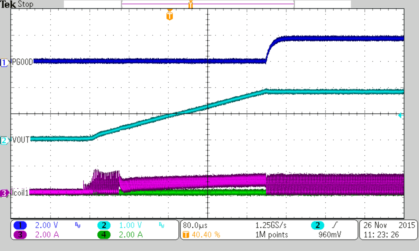
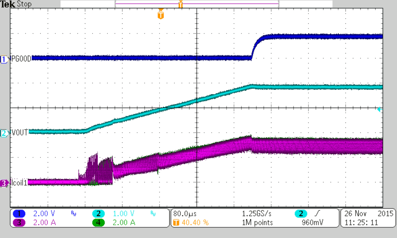
The soft start ramp time can be set externally connecting a capacitor between the SS/TR and AGND pins. The capacitor value CSS that is needed to get a specific rising time ΔtSS calculates as:
space

space
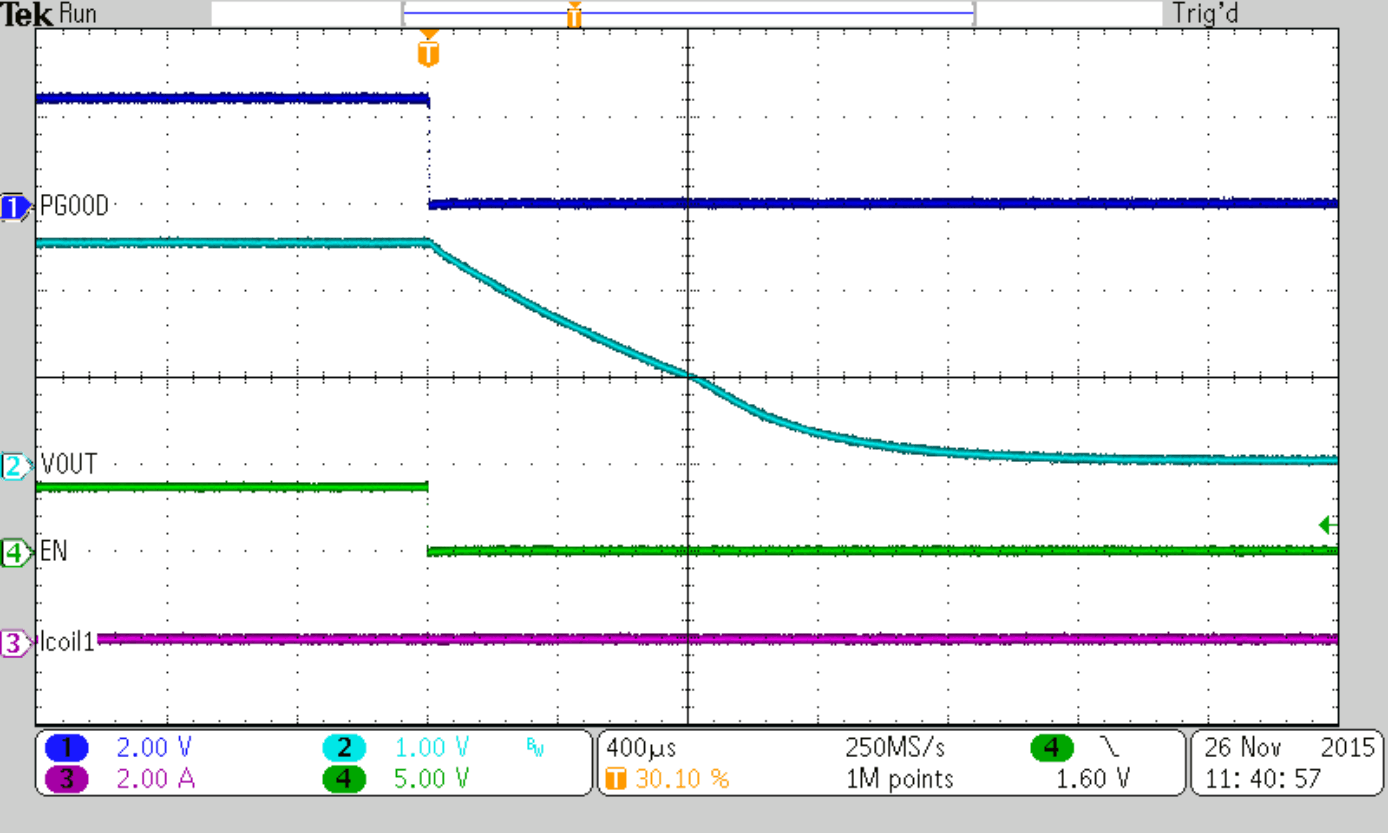
Since the device has an internal delay time ΔtDELAY from EN=High to start switching, the overall startup time is longer as shown in Figure 7.
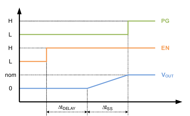 Figure 7. Soft Start ΔtSS
If very large output capacitances are used (e.g. >4x47µF), the use of a soft start capacitor is mandatory to secure complete startup.
8.2.2.8 Tracking
For values up to 0.6V, an external voltage, connected to the SS/TR pin, drives the voltage level at the FB pin. In doing so, the voltage at the FB pin is directly proportional to the voltage at the SS/TR pin.
When choosing the resistive divider proportion according to Equation 10, VOUT tracks VTR simultaneously.
space

space
space
Following the example of Setting the Adjustable Output Voltage with VOUT = 1.8 V, R1 = 240 kΩ and R2 = 120 kΩ, Equation 11 and Equation 12 calculate R3 and R4, connected to the SS/TR pin. Different to the resistive divider at the FB pin, a larger current must be chosen, to avoid a tracking offset caused by the 5.25 µA current that flows out of the SS/TR pin. Assuming a 250 µA current, R4 calculates as follows:
space

space
R3 calculates now rearranging Equation 10:
space

space
However, the following limitations can influence the tracking accuracy:
- The upper limit of the SS/TR voltage that can be tracked is about 0.6V. Since it is detected internally by a comparator, process variation and ramp speed can cause up to ±30 mV different threshold.
- In case that the voltage at SS/TR ramps up immediately when VIN is supplied or EN is set High, the internal startup delay, ΔtDELAY, delays the ramp of VOUT. The internal ramp starts after ΔtDELAY at the voltage level, which is actually present at the SS/TR pin.
- The tracking down speed is limited by the RC time constant of the internal output discharge (always connected when tracking down) and the actual load with the output capacitance. Note: The device tracks down with the same behavior for MODE High (Forced PWM) or Low (Auto PSM).
8.2.2.9 Current Sharing
The TPS62480 is designed to share load current wisely between the 2 phases. The current imbalance is less than 15% over VIN and temperature range and independent on inductor mismatch.
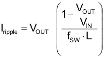
However, the mismatch between the two inductors itself causes additional imbalance of the average inductor currents, caused by different ripple current. The mismatch can be calculated as shown in the following example, assuming that the nominal inductance of 470 nH can vary ±20%, the switching frequency is 2 MHz. Converting 5 V into 2.5 V gives a duty cycle of 0.5, which effects maximum ripple current. Since the ripple current is calculated with:
space
space
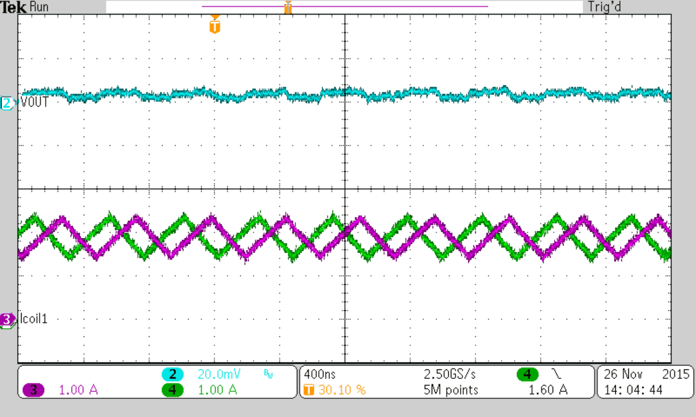
the ripple currents in the two inductors are calculated with Iripple1 = 1.69 A and Iripple2 = 1.1 A which gives a ΔIripple of 0.59 A as worst case number based on the maximum inductor tolerance. Figure 9 shows the relation of the two inductor currents in such case.
space

The difference in the average current is calculated using:
space

space
In this worst case calculation the average inductor current mismatch is 0.295A, less than 10% at the full load current of 3A per phase.
Thermal Good
The Thermal Good pin provides an open drain output. The logic level is given by the pull up source which can be VOUT. In this case, TG goes or stays Low, when the device switches off due to EN, UVLO or Thermal Shutdown.
When using an independent source for the pull up logic, the logic behavior at shutdown differs, because the TG pin internally goes high impedance. As before, TG goes Low when TG threshold is reached, but goes back High in the event of being switched off (e.g. Thermal Shutdown).
8.2.3 Application Curves
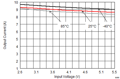
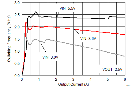
VIN= 3.6 V, VOUT = 1.8V (R1 / R2 = 240 kΩ / 120 kΩ), TA = 25°C, (unless otherwise noted)
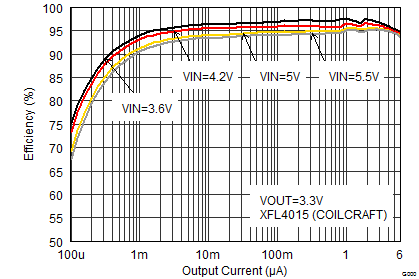
| VOUT = 3.3 V |
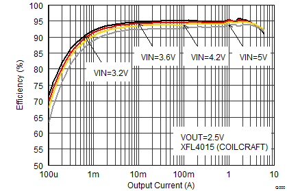
| VOUT = 2.5 V |
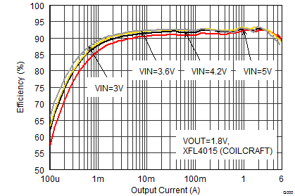
| VOUT = 1.8 V |
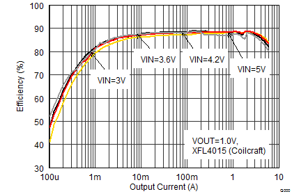
| VOUT = 1 V |
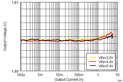
(Load Regulation)
| VOUT = 0.6 V |
| VOUT = 2.5 V |
| VOUT = 1.8 V | ||
| VOUT = 2.5 V | ||
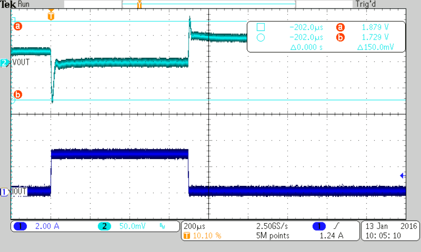
Load Step 0 to 3 A
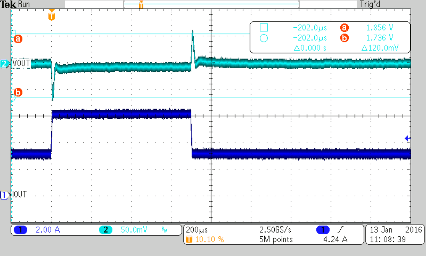
Load Step 3 to 6 A
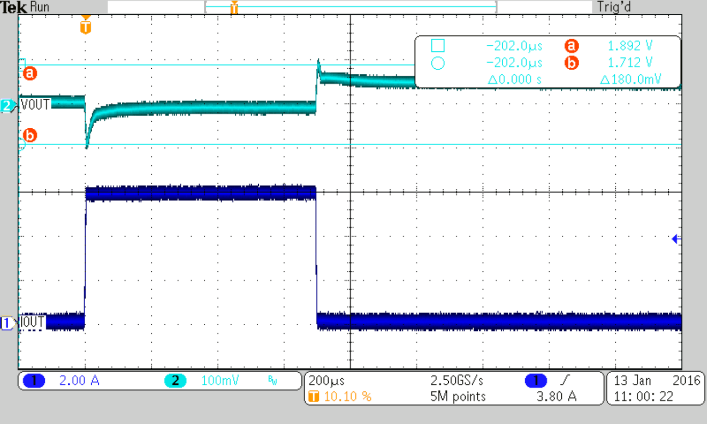
| Cff = 36 pF (nom) | ||
Load Step 0 to 6 A
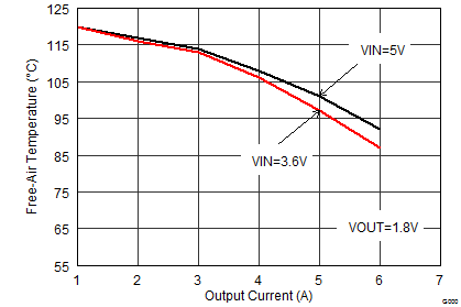 Figure 38. Maximum Ambient Temperature
(TPS62480 EVM)
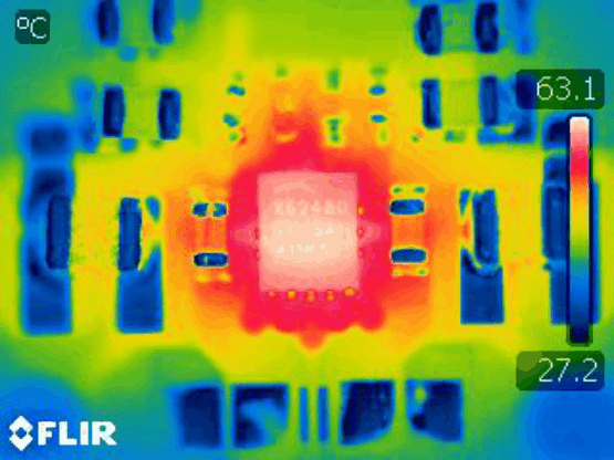
| VIN = 3.6 V | VOUT = 1.8 V | IOUT = 6 A |
| TA = 25°C |
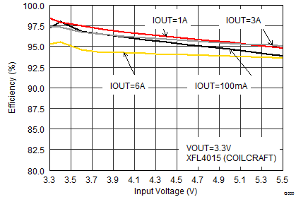
| VOUT = 3.3 V |
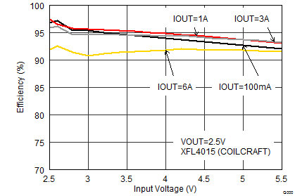
| VOUT = 2.5 V |
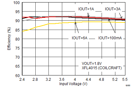
| VOUT = 1.8 V |
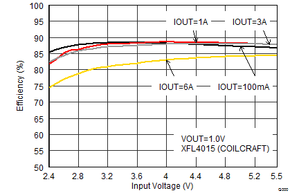
| VOUT = 1 V |
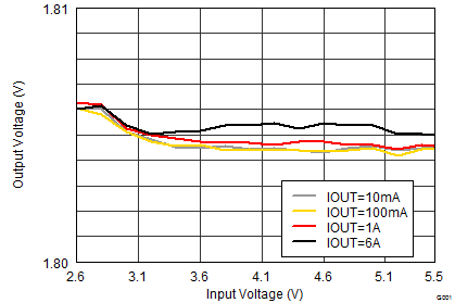
(Line Regulation)
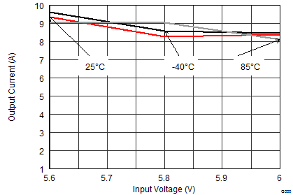
| VOUT = 5.5 V |
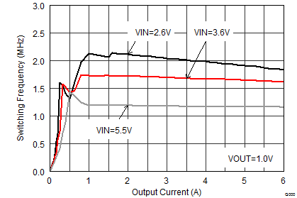
| VOUT = 1 V |
| VOUT = 1.8 V | ||
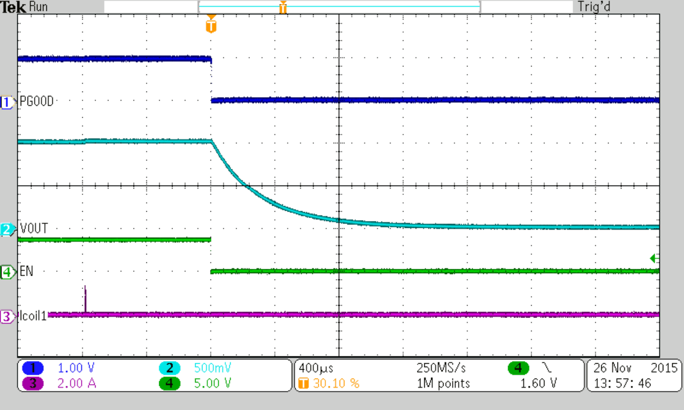
| VOUT = 1 V | ||
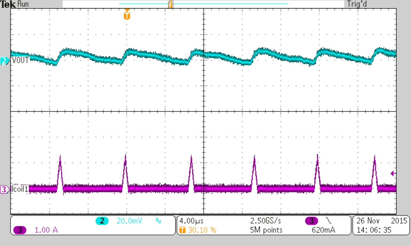
| IOUT = 50 mA | ||
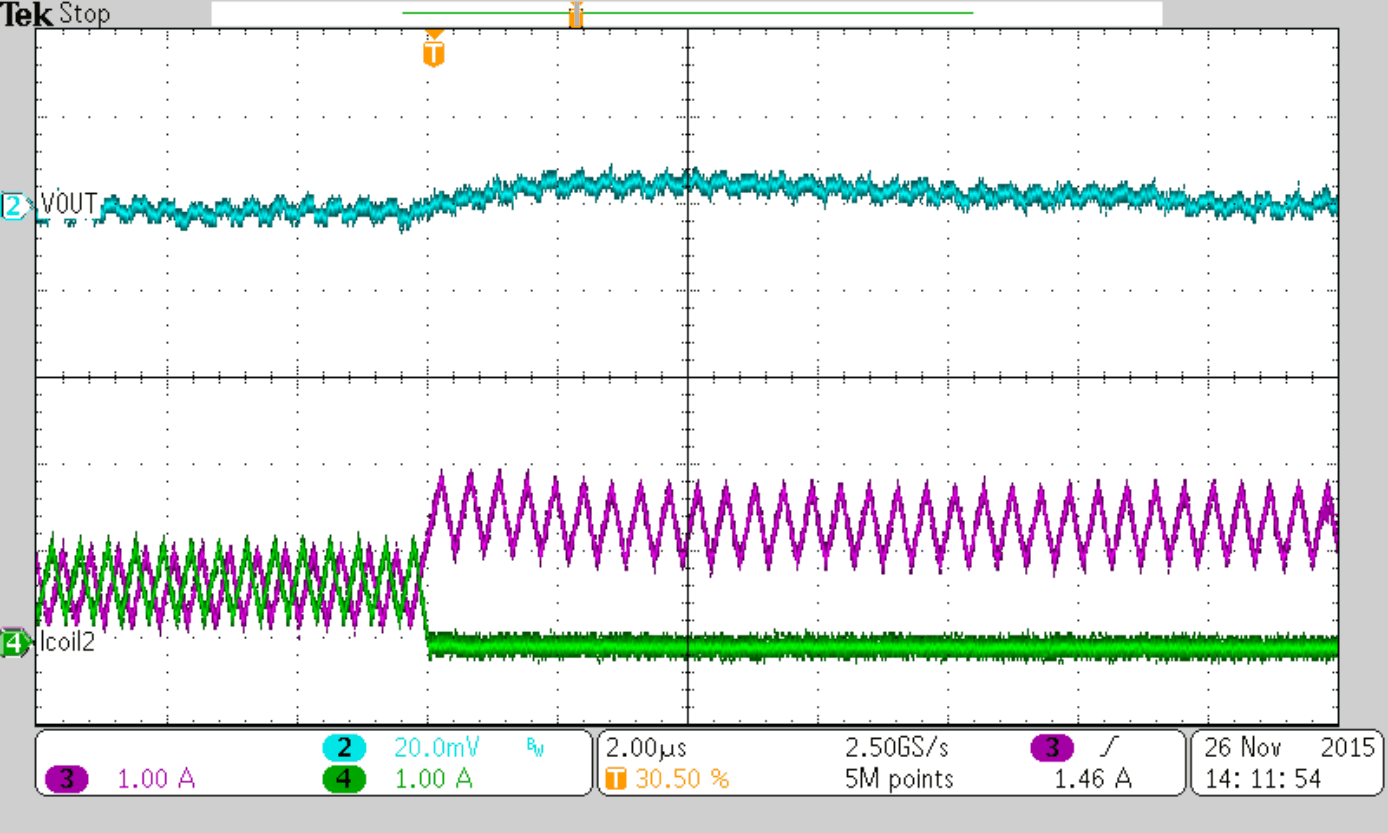
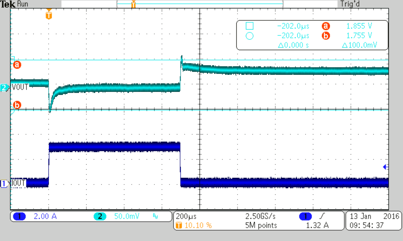
| Cff = 36 pF (nom) | ||
Load Step 0 to 3 A
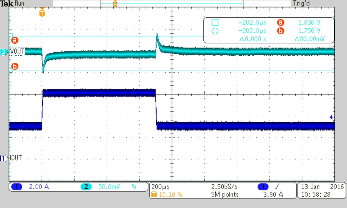
| Cff = 36 pF (nom) | ||
Load Step 3 to 6 A
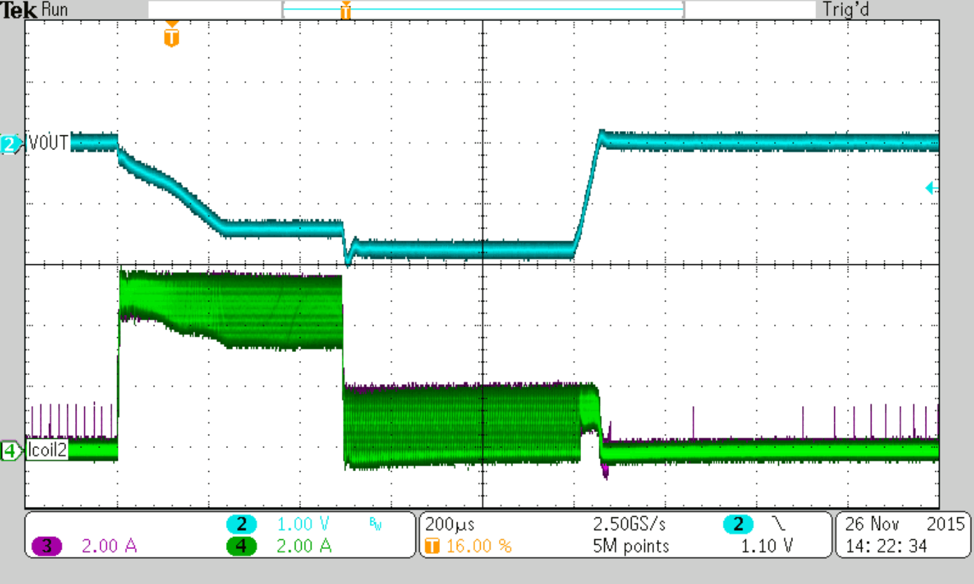
| IOUT = 10 A | ||
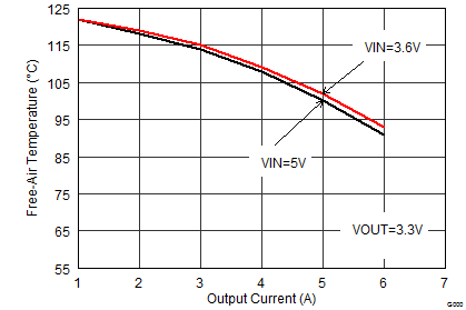 Figure 39. Maximum Ambient Temperature
(TPS62480 EVM)
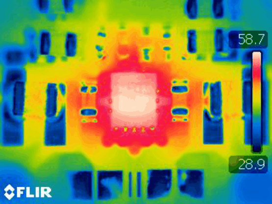
| VIN = 5 V | VOUT = 3.3 V | IOUT = 6 A |
| TA = 25°C |
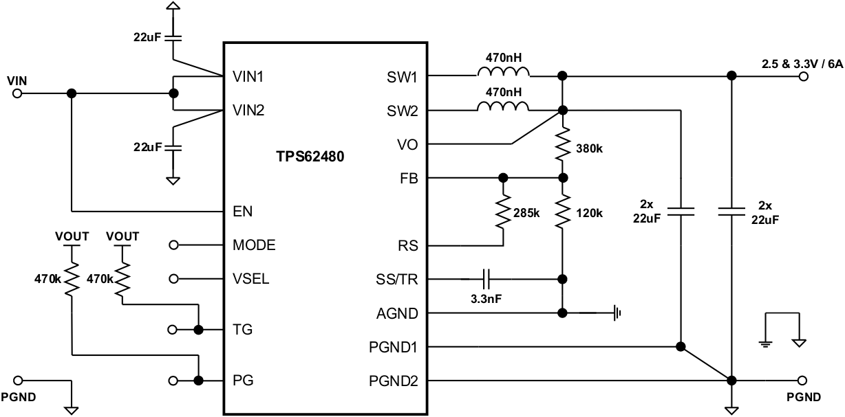
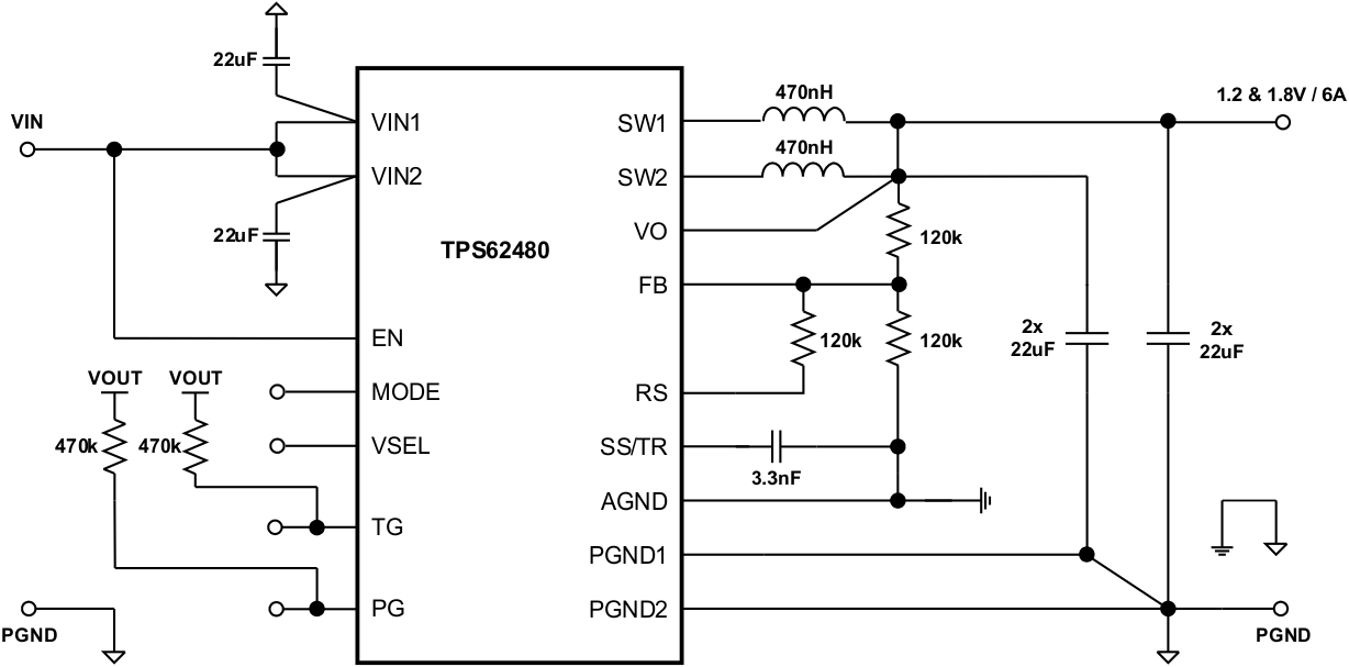
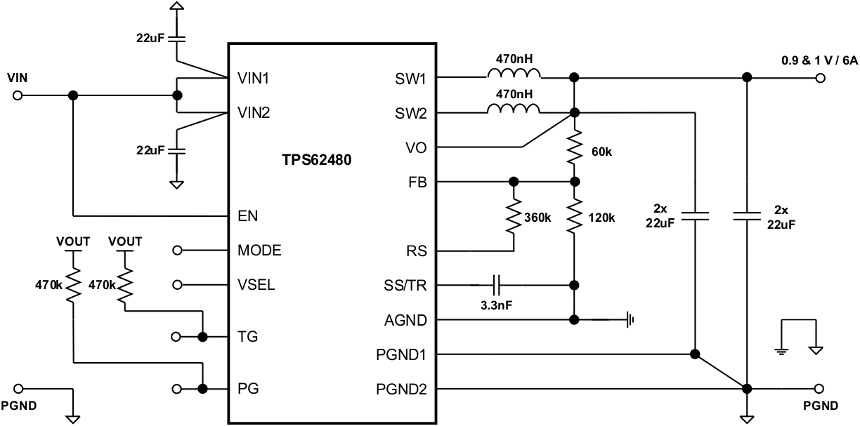
8.3 System Examples
This section provides typical schematics for commonly used output voltages values.
space
space
space

space
space
space