SLVSAO5B December 2010 – October 2015 TPS62590-Q1
PRODUCTION DATA.
- 1 Features
- 2 Applications
- 3 Description
- 4 Revision History
- 5 Pin Configuration and Functions
- 6 Specifications
- 7 Parameter Measurement Information
- 8 Detailed Description
- 9 Application and Implementation
- 10Power Supply Recommendations
- 11Layout
- 12Device and Documentation Support
- 13Mechanical, Packaging, and Orderable Information
1 Features
- Qualified for Automotive Applications
- Output Current up to 1000 mA
- Input Voltage Range from 2.5 V to 6 V
- High Efficiency Step Down Converter
- Output Voltage Accuracy in PWM mode ±2.5%
- Typical 15-μA Quiescent Current
- 2.25 MHz Fixed Frequency Operation
- Power Save Mode at Light Load Currents
- 100% Duty Cycle for Lowest Dropout
2 Applications
- Automotive Infotainment and Cluster
- Head Unit
- Navigation
- Display
- Advanced Driver Assistance System (ADAS)
- Front Cameras
- Blind Spot Monitoring
- Lane Departure Warning
- Park Assist
3 Description
The TPS62590-Q1 device is a high-efficiency synchronous step-down converter, optimized for space constrained applications and very low quiescent current requirements. It provides up to 1000-mA output current from preregulated low voltage rails and consumes 15 uA (typical) in power-save mode.
With an input voltage range of 2.5 V to 6 V and an output voltage accuracy of 2.5%, the device is targeted to power a large variety of automotive applications.
The TPS62590-Q1 family operates at a 2.25-MHz fixed switching frequency and enters a power-save mode at light load currents to maintain a high efficiency over the entire load current range.
The power-save mode is optimized for low output-voltage ripple. For low-noise applications, the device can be forced into fixed-frequency PWM mode by pulling the MODE pin high. In the shutdown mode, the current consumption is reduced to less than 1 µA. The TPS62590-Q1 allows the use of small inductors and capacitors to achieve a small solution size.
The TPS62590-Q1 is available in a 2-mm × 2-mm
6-pin SON package with a thermal pad for improved thermal performance.
Device Information(1)
| PART NUMBER | PACKAGE | BODY SIZE (NOM) |
|---|---|---|
| TPS62590-Q1 | SON (6) | 2.00 mm × 2.00 |
- For all available packages, see the orderable addendum at the end of the data sheet.
Typical Application Schematic

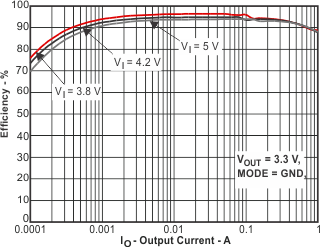
Efficiency vs Load Current
