ZHCSE11A June   2015  – June 2015 TPS62745 , TPS627451

PRODUCTION DATA.  

  1. 特性
  2. 应用
  3. 说明
  4. 典型应用电路原理图
  5. 修订历史记录
  6. Device Comparison Table
  7. Pin Configuration and Functions
  8. Specifications
    1. 8.1 Absolute Maximum Ratings
    2. 8.2 ESD Ratings
    3. 8.3 Recommended Operating Conditions
    4. 8.4 Thermal Information
    5. 8.5 Electrical Characteristics
    6. 8.6 Timing Characteristics
    7. 8.7 Typical Characteristics
  9. Detailed Description
    1. 9.1 Overview
    2. 9.2 Functional Block Diagram
    3. 9.3 Feature Description
      1. 9.3.1 DCS-Control™
      2. 9.3.2 Enable / Shutdown
      3. 9.3.3 Power Good Output (PG)
      4. 9.3.4 Output Voltage Selection (VSEL1 - 4)
      5. 9.3.5 Input Voltage Switch
    4. 9.4 Device Functional Modes
      1. 9.4.1 Soft Start
    5. 9.5 VOUT Discharge
    6. 9.6 Internal Current Limit
  10. 10Application and Implementation
    1. 10.1 Application Information
    2. 10.2 Typical Application
      1. 10.2.1 Design Requirements
      2. 10.2.2 Detailed Design Procedure
        1. 10.2.2.1 Output Voltage Selection (VSEL1 - 4)
        2. 10.2.2.2 Output Filter Design (Inductor and Output Capacitor)
        3. 10.2.2.3 Inductor Selection
        4. 10.2.2.4 DC/DC Output Capacitor Selection
        5. 10.2.2.5 Input Capacitor Selection
      3. 10.2.3 Application Curves
    3. 10.3 System Examples
      1. 10.3.1 TPS62745 Set to a Fixed Voltage of 3.3 V
        1. 10.3.1.1 Design Requirements
        2. 10.3.1.2 Detailed Design Procedure
        3. 10.3.1.3 Application Curves
      2. 10.3.2 Dynamic Voltage Change on TPS62745
        1. 10.3.2.1 Design Requirements
        2. 10.3.2.2 Detailed Design Procedure
        3. 10.3.2.3 Application Curves
  11. 11Power Supply Recommendations
  12. 12Layout
    1. 12.1 Layout Guidelines
    2. 12.2 Layout Example
  13. 13器件和文档支持
    1. 13.1 器件支持
      1. 13.1.1 Third-Party Products Disclaimer
    2. 13.2 相关链接
    3. 13.3 社区资源
    4. 13.4 商标
    5. 13.5 静电放电警告
    6. 13.6 Glossary
  14. 14机械、封装和可订购信息

封装选项

机械数据 (封装 | 引脚)
散热焊盘机械数据 (封装 | 引脚)
订购信息

12 Layout

12.1 Layout Guidelines

As for all switching power supplies, the layout is an important step in the design. Especially RF designs demand careful attention to the PCB layout. Care must be taken in board layout to get the specified performance. If the layout is not carefully done, the regulator could show poor line and/or load regulation, stability issues as well as EMI problems and interference with RF circuits. It is critical to provide a low inductance, impedance ground path. Therefore, use wide and short traces for the main current paths. The input capacitor should be placed as close as possible to the IC pins as well as the inductor and output capacitor. Use a common power GND node and a different node for the signal GND to minimize the effects of ground noise. Keep the common path to the GND pin, which returns the small signal components and the high current of the output capacitors as short as possible to avoid ground noise. The VOUT line should be connected to the output capacitor and routed away from noisy components and traces (e.g. SW line).

12.2 Layout Example
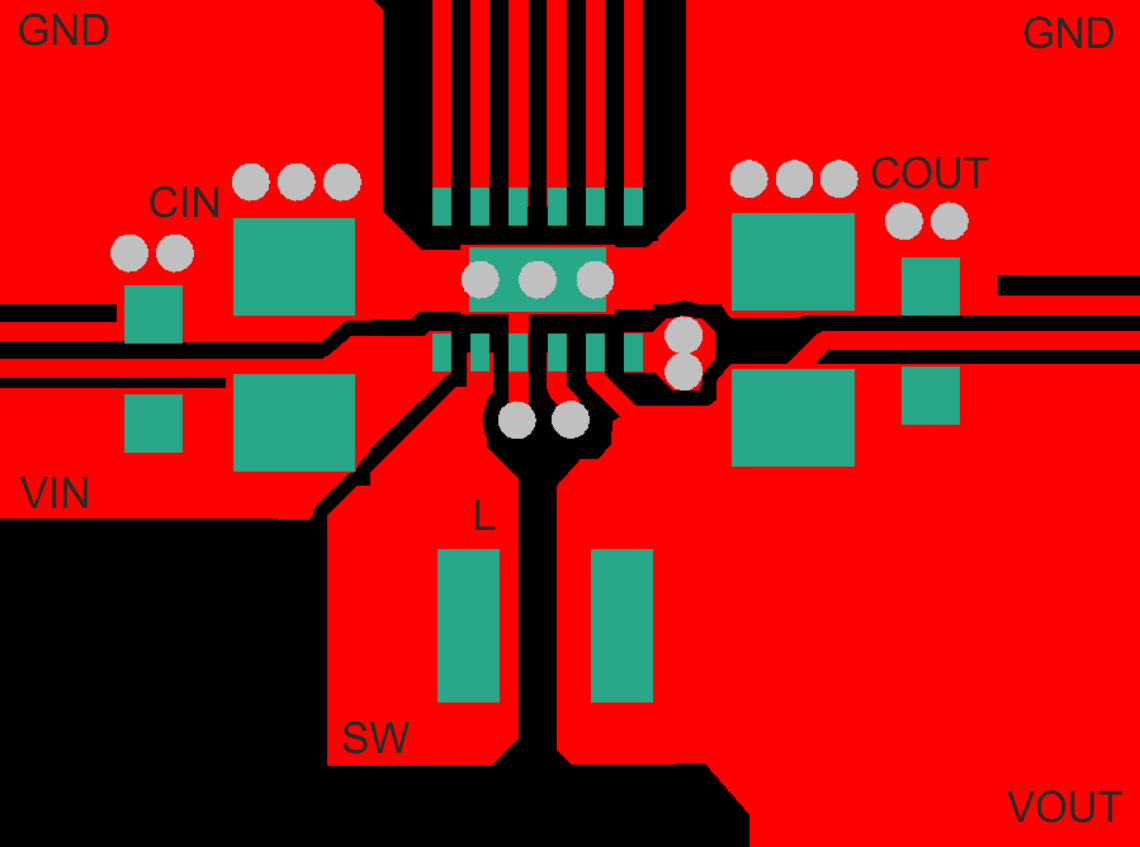
TPS62745 TPS627451 TPS62745layout.gif Figure 40. Recommended PCB Layout