ZHCSE11A June 2015 – June 2015 TPS62745 , TPS627451
PRODUCTION DATA.
- 1 特性
- 2 应用
- 3 说明
- 4 典型应用电路原理图
- 5 修订历史记录
- 6 Device Comparison Table
- 7 Pin Configuration and Functions
- 8 Specifications
- 9 Detailed Description
- 10Application and Implementation
- 11Power Supply Recommendations
- 12Layout
- 13器件和文档支持
- 14机械、封装和可订购信息
10 Application and Implementation
10.1 Application Information
The TPS62745 devices are a step down converter family featuring typical 400-nA quiescent current and operating with a tiny 4.7-μH inductor and a 10-μF output capacitor. These DCS-Control™ based devices extend the light load efficiency range below 10-μA load currents. TPS62745 supports output currents up to 300 mA,
10.2 Typical Application
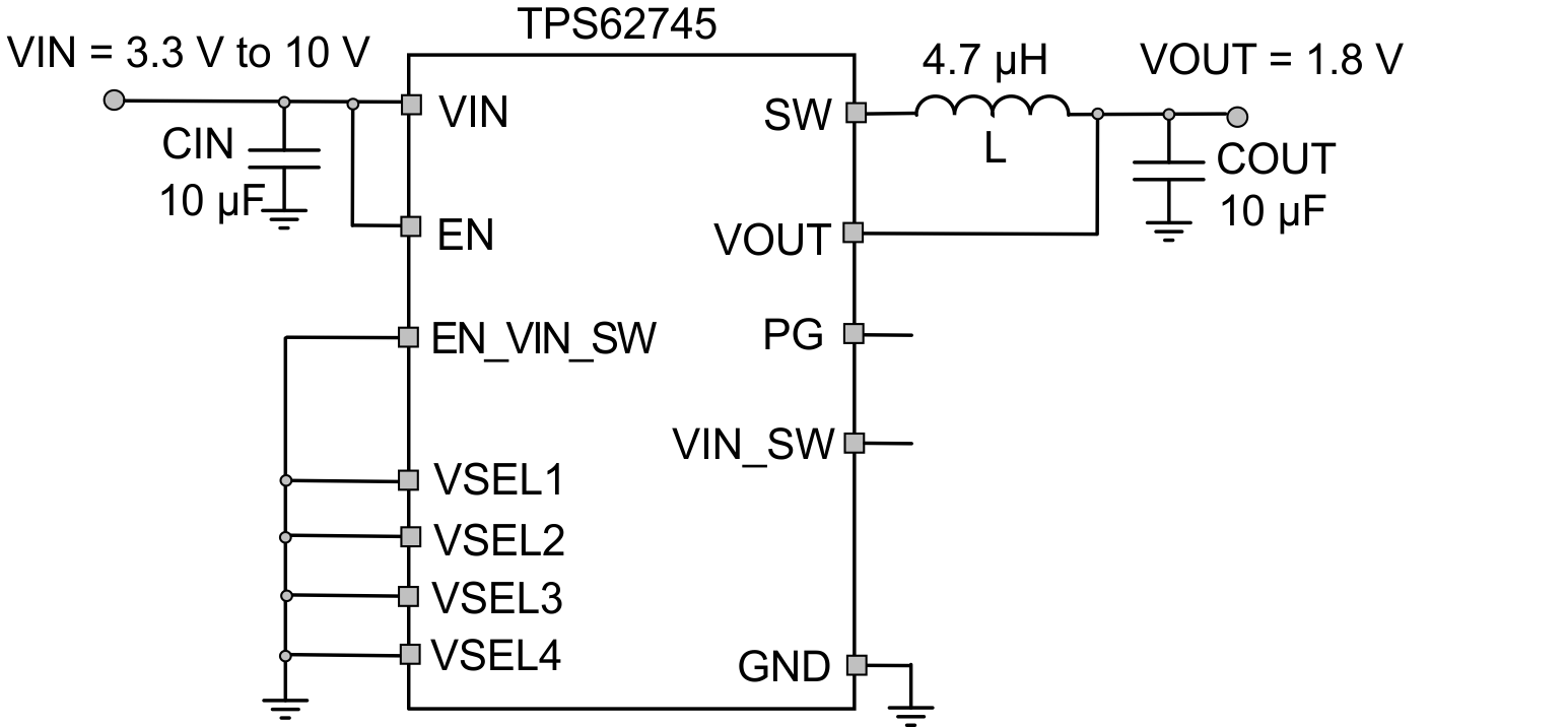 Figure 5. TPS62745 Typical Application
10.2.1 Design Requirements
The TPS62745 is a highly integrated DC/DC converter. The output voltage is set via the VSEL pin interface without any additional external components. For proper operation only an input and output capacitor and an inductor is required. When the input voltage switch is not used, its enable input should be tied to GND. The output VIN_SW can either be left open or tied to GND. Table 3 shows the components used for the application characteristic curves.
Table 3. List of Components
| REFERENCE | DESCRIPTION | Value | MANUFACTURER(1) |
|---|---|---|---|
| IC | TPS62745 | Texas Instruments | |
| L | DFE252010 | 4.7 µH | Toko |
| CIN | TMK212BBJ106MG | 10 µF / 25 V / X5R / 0805 | Taiyo Yuden |
| COUT | LMK212ABJ106KG-T | 10 µF / 10 V / X5R / 0805 | Taiyo Yuden |
10.2.2 Detailed Design Procedure
10.2.2.1 Output Voltage Selection (VSEL1 - 4)
The VSEL pins select the output voltage of the converters. See the Output Voltage Selection (VSEL1 - 4) of the Feature Descriptions. The output voltage can be changed during operation by changing the logic level of these pins. The output voltage of the TPS62745 ramps to the new target with a slew rate as defined in the electrical characteristics. Typically these pins are driven by an applications processor with an I/O voltage of either 1.8 V or 3.3 V or hard wired to a logic high or logic low signal. In case the pins are not driven from an applications processor and the supply voltage is higher than the voltage rating of the VSEL pins, a logic high level can be taken from the output voltage at pin VOUT. During start-up, when the output is rising from 0 V to its target, the VSEL pins connected to VOUT will change their logic level from low to high. TPS62745 is designed such that such a configuration ensures a steadily rising output voltage.
10.2.2.2 Output Filter Design (Inductor and Output Capacitor)
The external components have to fulfill the needs of the application, but also the stability criteria of the devices control loop. The TPS62745 is optimized to work within a range of L and C combinations. The LC output filter inductance and capacitance have to be considered together, creating a double pole, responsible for the corner frequency of the converter. Table 4 can be used to simplify the output filter component selection.
Table 4. Recommended LC Output Filter Combinations
| Inductor Value [µH](2) | Output Capacitor Value [µF](1) | |
|---|---|---|
| 10 µF | 22 µF | |
| 4.7 | √(3) | √ |
| 3.3 | √ | √ |
10.2.2.3 Inductor Selection
The inductor value affects its peak-to-peak ripple current, the PWM-to-PFM transition point, the output voltage ripple and the efficiency. The selected inductor has to be rated for its DC resistance and saturation current. The inductor ripple current (ΔIL) decreases with higher inductance and increases with higher VIN or VOUT and can be estimated according to Equation 1.
Equation 2 calculates the maximum inductor current under static load conditions. The saturation current of the inductor should be rated higher than the maximum inductor current as calculated with Equation 2. This is recommended because during heavy load transient the inductor current will rise above the calculated value. A more conservative way is to select the inductor saturation current according to the high-side MOSFET switch current limit ILIMF.


where
- f = Switching frequency
- L = Inductor value
- ΔIL= Peak-to-peak inductor ripple current
- ILmax = Maximum inductor current
In DC/DC converter applications, the efficiency is essentially affected by the inductor AC resistance (i.e. quality factor) and by the inductor DCR value. To achieve high efficiency operation, care should be taken in selecting inductors featuring a quality factor above 25 at the switching frequency. Increasing the inductor value produces lower RMS currents, but degrades transient response. For a given physical inductor size, increased inductance usually results in an inductor with lower saturation current.
The total losses of the coil consist of both the losses in the DC resistance RDC) and the following frequency-dependent components:
- The losses in the core material (magnetic hysteresis loss, especially at high switching frequencies)
- Additional losses in the conductor from the skin effect (current displacement at high frequencies)
- Magnetic field losses of the neighboring windings (proximity effect)
- Radiation losses
The following inductor series from different suppliers have been used:
Table 5. List of Inductors
| INDUCTANCE [µH] | DCR [Ω], typical | DIMENSIONS [mm3] | INDUCTOR TYPE | SUPPLIER(1) |
|---|---|---|---|---|
| 4.7 | 0.250 | 2.5 x 2.0 x 1.0 | DFE252010 | TOKO |
| 3.3 | 0.190 | 2.5 x 2.0 x 1.0 | DFE252010 | TOKO |
| 4.7 | 0.336 | 2.0 x 1.9 x 1.0 | XPL2010 | Coilcraft |
| 3.3 | 0.207 | 2.0 x 1.9 x 1.0 | XPL2010 | Coilcraft |
| 4.7 | 0.217 | 3.0 x 3.0 x 1.1 | XFL3010 | Coilcraft |
| 4.7 | 0.270 | 4.5 x 3.2 x 3.2 | CC453232 | Bourns |
10.2.2.4 DC/DC Output Capacitor Selection
The DCS-Control™ scheme of the TPS62745 allows the use of tiny ceramic capacitors. Ceramic capacitors with low ESR values have the lowest output voltage ripple and are recommended. The output capacitor requires either an X7R or X5R dielectric. Y5V and Z5U dielectric capacitors, aside from their wide variation in capacitance over temperature, become resistive at high frequencies. At light load currents, the converter operates in power save mode and the output voltage ripple is dependent on the output capacitor value and the PFM peak inductor current. A larger output capacitor can be used, but it should be considered that larger output capacitors lead to an increased leakage current in the capacitor and may reduce overall conversion efficiency. Furthermore, larger output capacitors impact the start up behavior of the DC/DC converter. Furthermore, the contol loop of the TPS62745 requires a certain voltage ripple across the output capacitor. Super-capacitors can be used in parallel to the ceramic capacitors when it is made sure that the super-capacitors series resistance is large enough to provide a valid feedback signal to the error amplifier which is in phase with the inductor current. Applications using an output capacitance above of what is stated under Recommended Operating Conditions should be checked for stability over the desired operating conditions range.
10.2.2.5 Input Capacitor Selection
Because of the nature of the buck converter having a pulsating input current, a low ESR input capacitor is required for best input voltage filtering to ensure proper function of the device and to minimize input voltage spikes. For most applications a 10 µF or 4.7 µF ceramic capacitor is recommended. The input capacitor can be increased without any limit for better input voltage filtering.
Table 6 shows a list of tested input/output capacitors.
Table 6. List of Input and Output Capacitors
| CAPACITANCE [μF] | SIZE | CAPACITOR TYPE | SUPPLIER(1) |
|---|---|---|---|
| 10 | 0603 | GRM188R61C106MA73 | Murata |
| 10 | 0603 | EMK107BBJ106MA | Taiyo Yuden |
| 4.7 | 0805 | EMK212ABJ475KG | Taiyo Yuden |
| 10 | 0805 | TMK212BBJ106MG | Taiyo Yuden |
| 10 | 0805 | LMK212ABJ106KG-T | Taiyo Yuden |
10.2.3 Application Curves
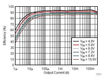
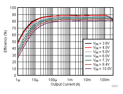
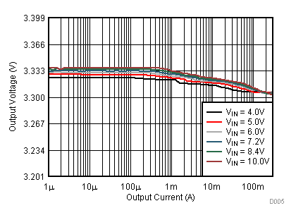
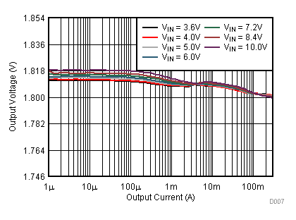


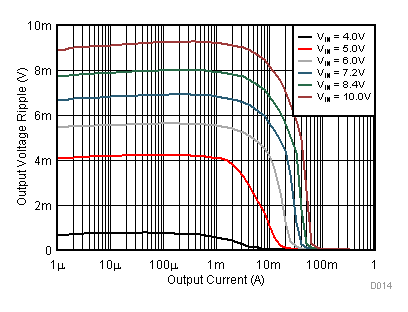
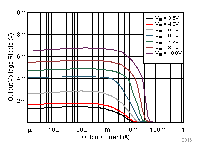
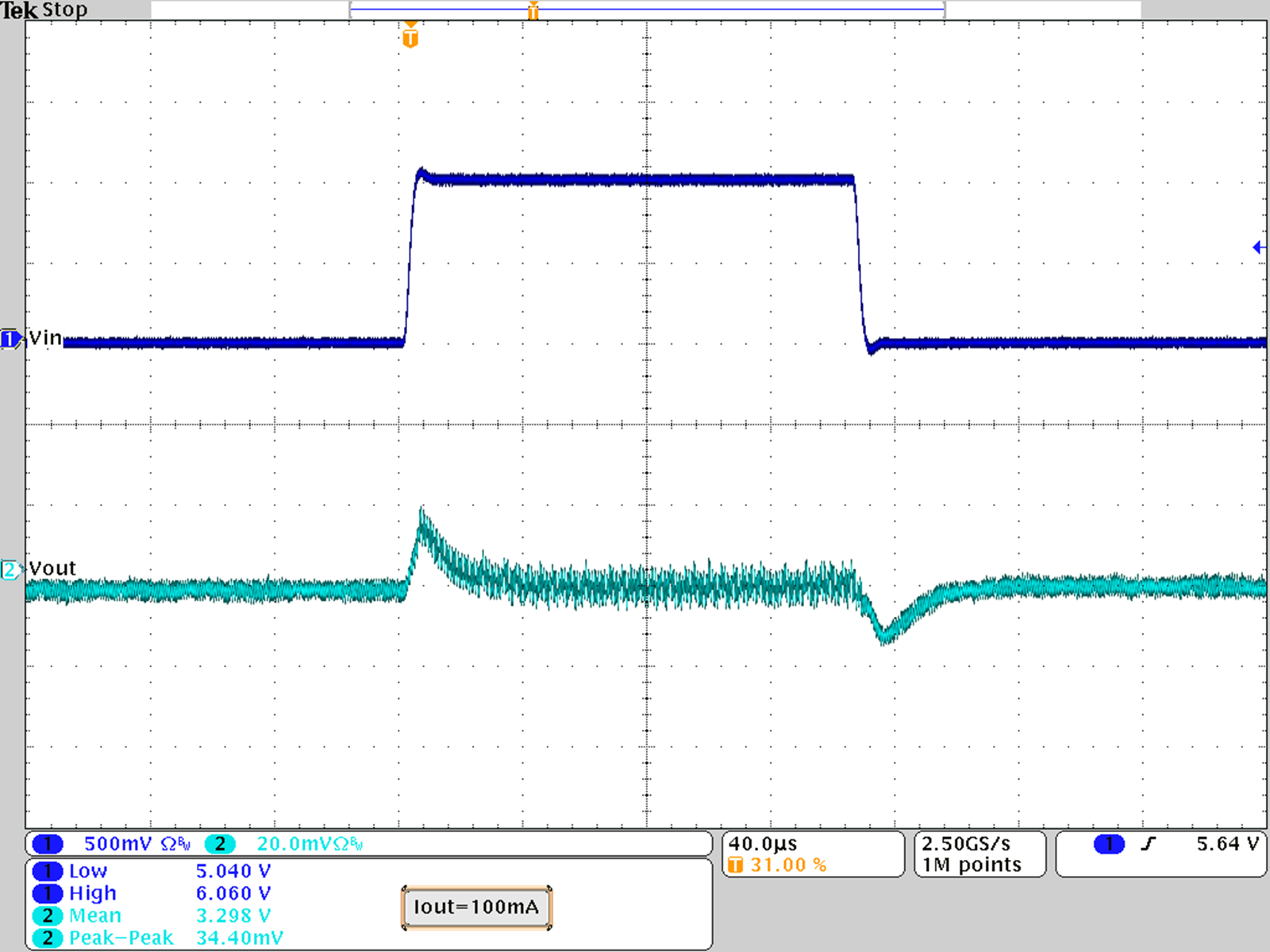 Figure 22. Line Transient Response; VOUT = 3.3 V
 Figure 24. Line Transient Response; VOUT = 1.8 V
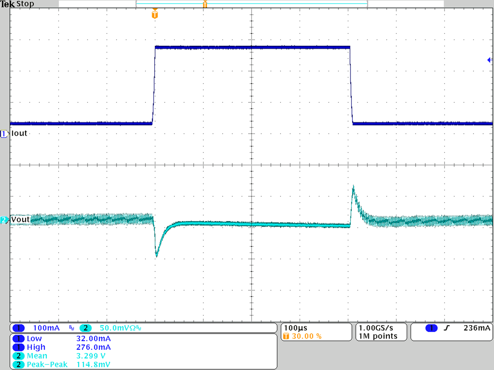 Figure 26. Load Transient Response; VOUT = 3.3 V
 Figure 28. Load Transient Response; VOUT = 1.8 V
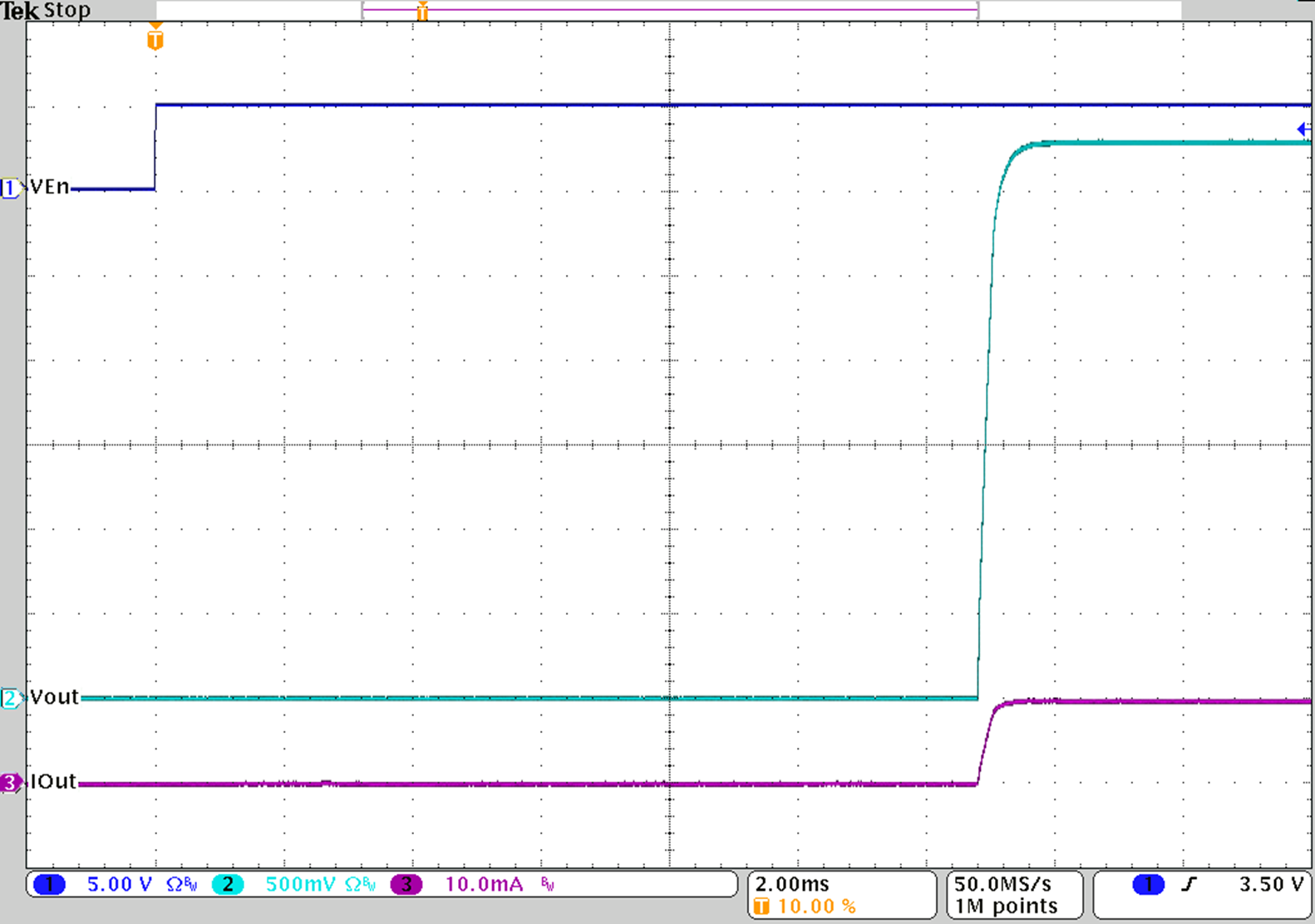 Figure 30. Startup with VOUT = 3.3 V
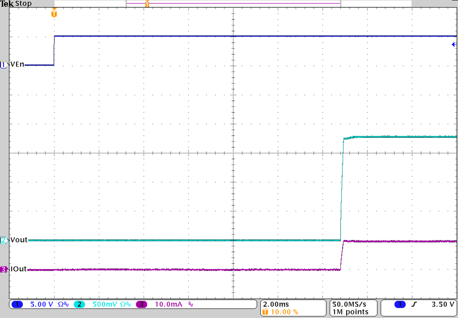 Figure 32. Startup with VOUT = 1.8 V
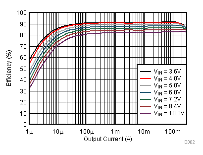
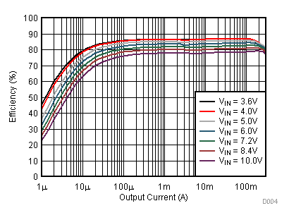
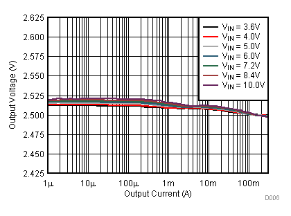
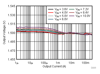

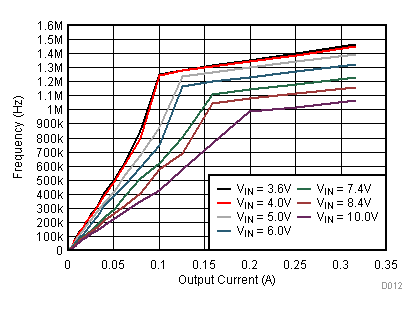
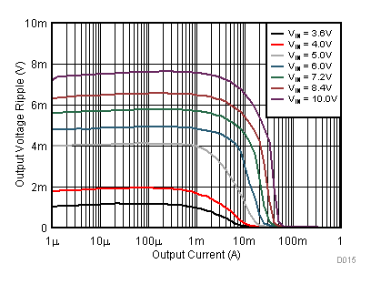
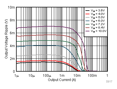
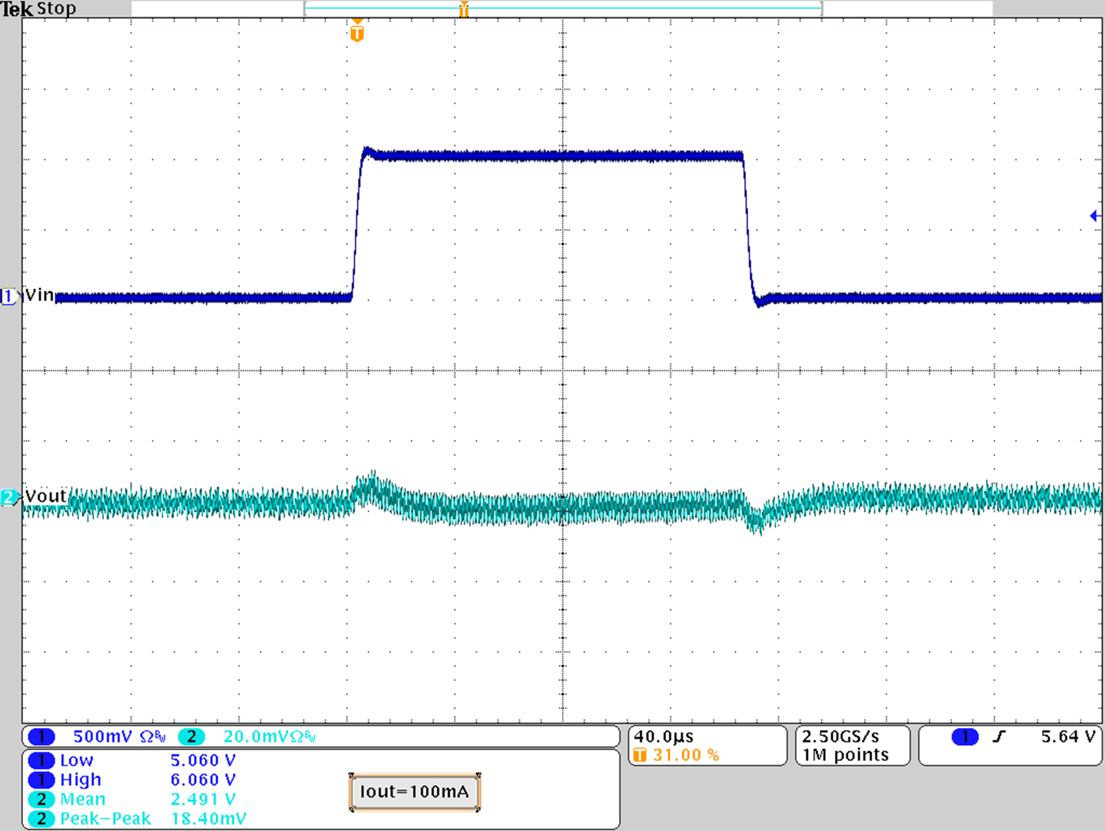 Figure 23. Line Transient Response; VOUT = 2.5 V
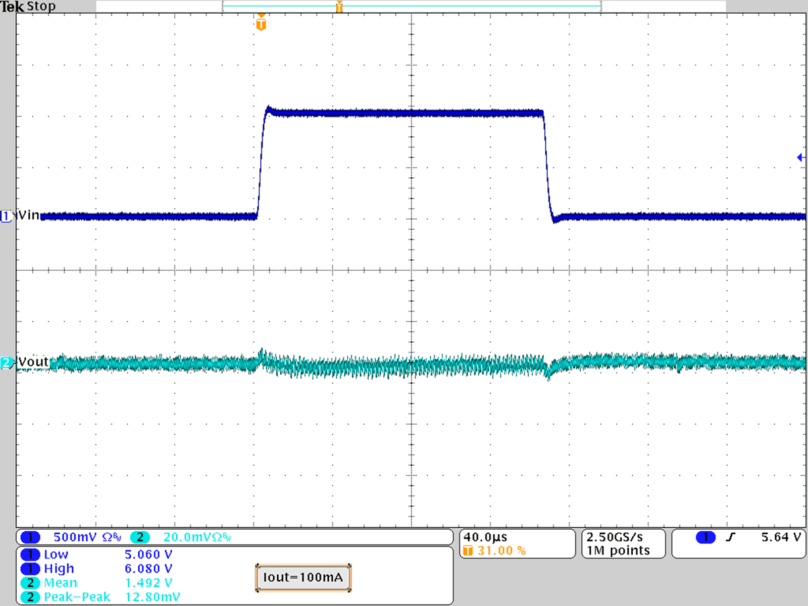 Figure 25. Line Transient Response; VOUT = 1.5 V
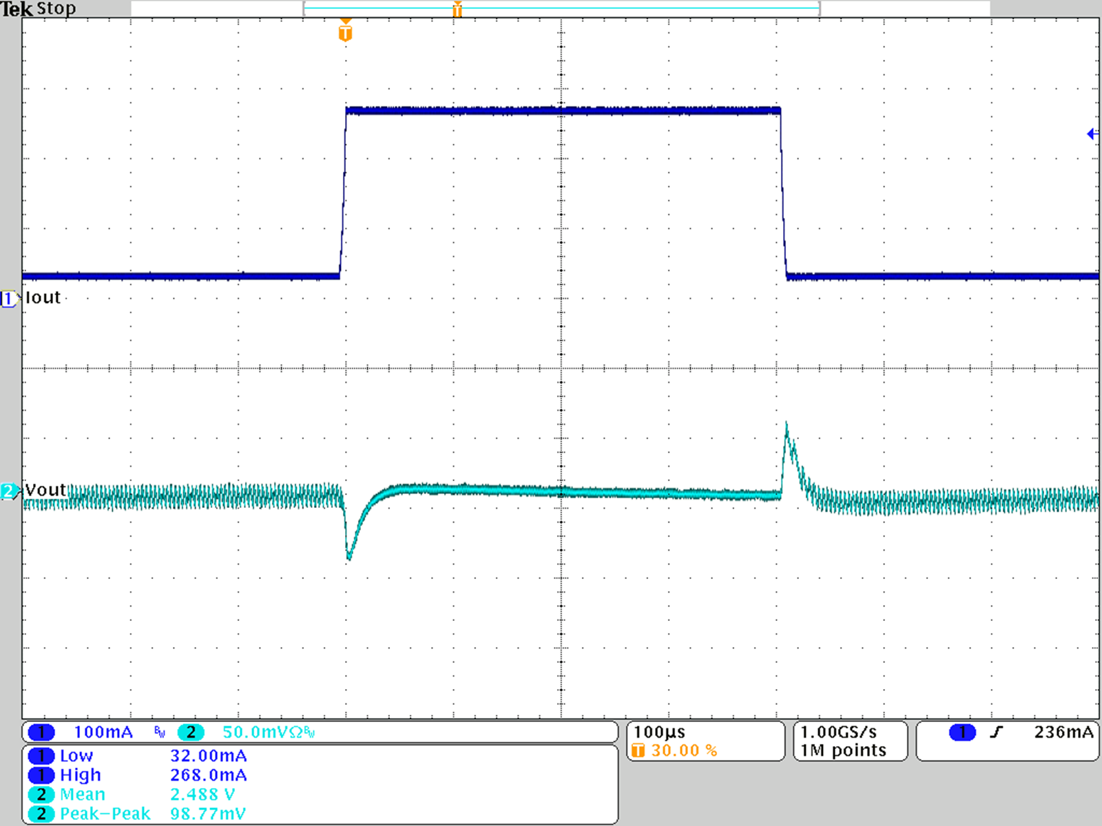 Figure 27. Load Transient Response; VOUT = 2.5 V
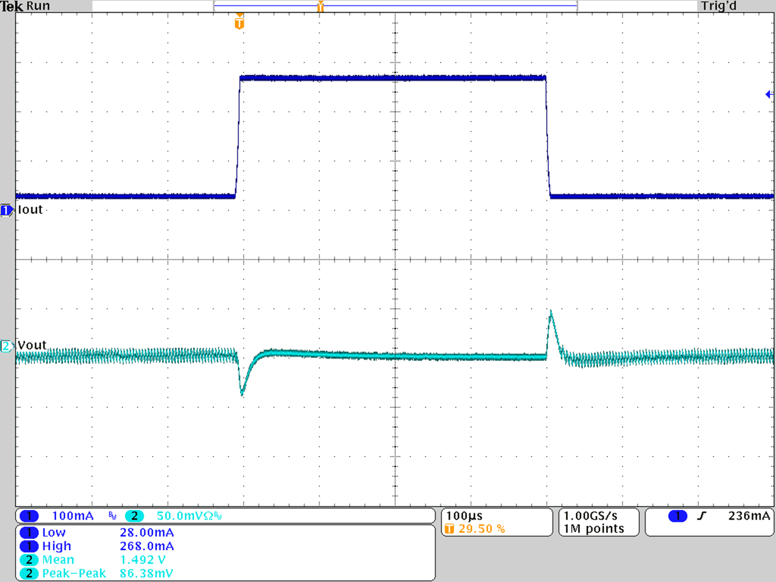 Figure 29. Load Transient Response; VOUT = 1.5 V
 Figure 31. Startup with VOUT = 2.5 V
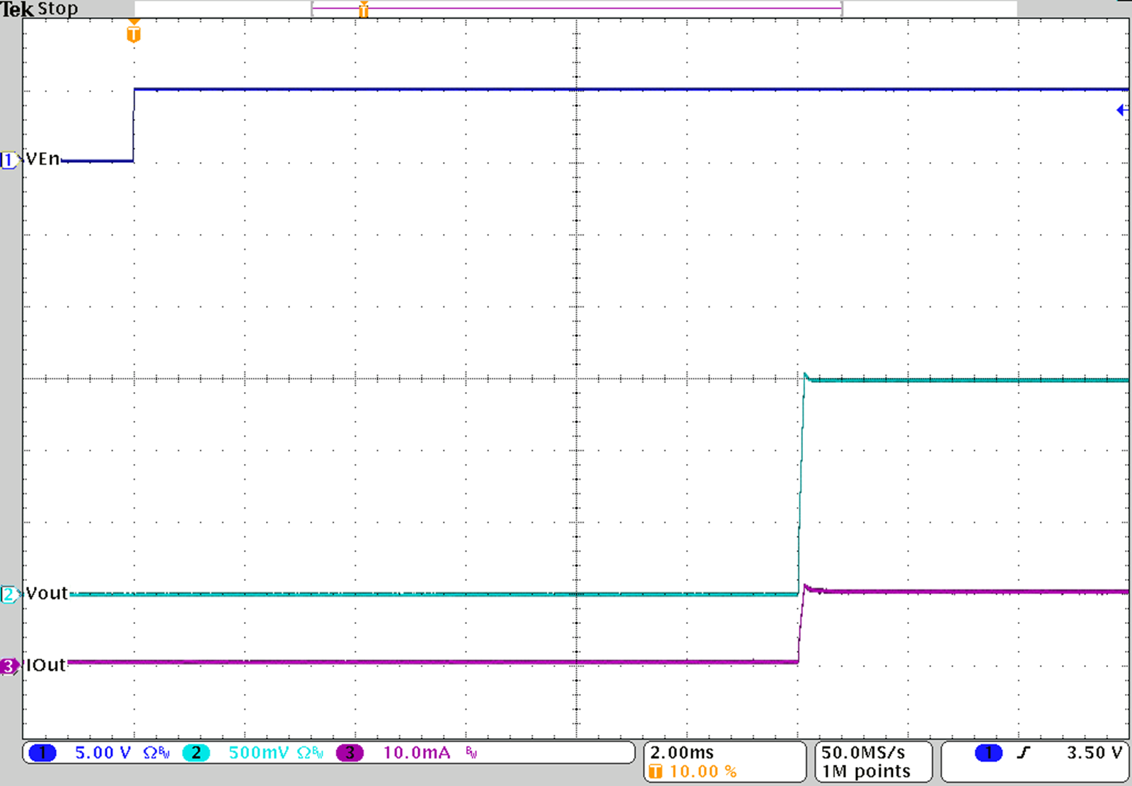 Figure 33. Startup with VOUT = 1.5 V
10.3 System Examples
10.3.1 TPS62745 Set to a Fixed Voltage of 3.3 V
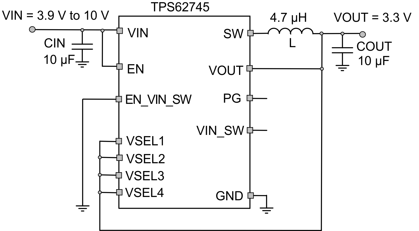 Figure 34. TPS62745 Typical Application for Vout = 3.3 V
10.3.1.1 Design Requirements
The minimum input voltage needs to be at least 700 mV above the desired output voltage for full output current.
Table 7. List of Components
| REFERENCE | DESCRIPTION | Value | MANUFACTURER(1) |
|---|---|---|---|
| IC | TPS62745 | Texas Instruments | |
| L | DFE252010 | 4.7 µH | Toko |
| CIN | TMK212BBJ106MG | 10 µF / 25 V / X5R / 0805 | Taiyo Yuden |
| COUT | LMK212ABJ106KG-T | 10 µF / 10 V / X5R / 0805 | Taiyo Yuden |
10.3.1.2 Detailed Design Procedure
The logic level of the VSEL pins sets the output voltage. The maximum high level does not allow a direct connection to the supply voltage if it is above 6 V. The output voltage can be used instead to provide a logic high level.
10.3.1.3 Application Curves
 Figure 35. TPS62745 with VOUT = 3.3 V Startup
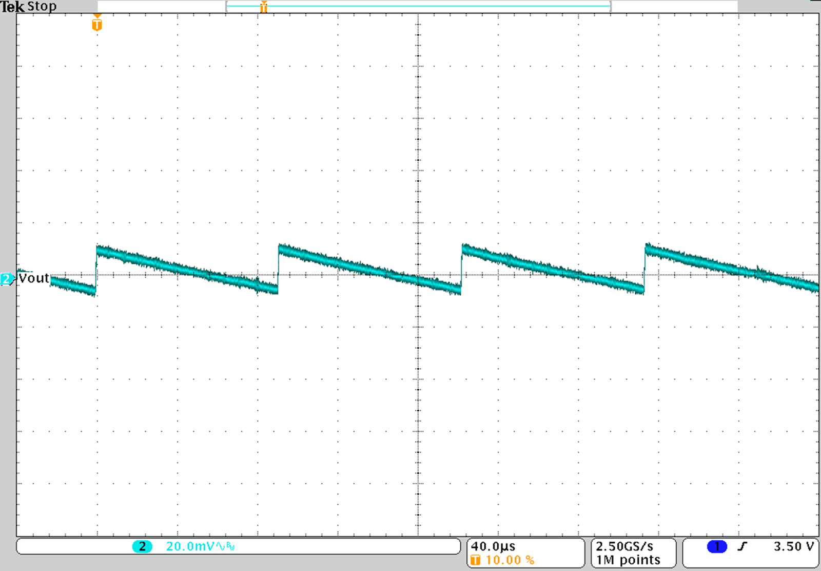 Figure 36. TPS62745 with VOUT = 3.3 V; Output Voltage Ripple for IOUT = 1 mA
10.3.2 Dynamic Voltage Change on TPS62745
TPS62745 allows to change its output voltage during operation by changing the logic level of the VSEL pins.
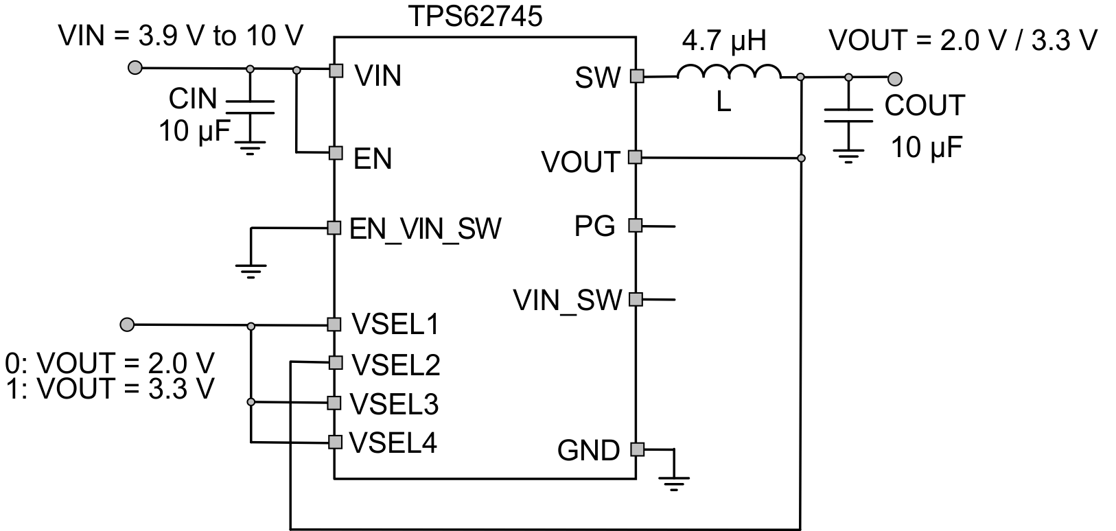 Figure 37. TPS62745 Typical Application for Switching Between Two Output Voltages
10.3.2.1 Design Requirements
The minimum input voltage needs to be at least 700 mV above the maximum output voltage for full output current. For an input voltage above 6V, the VSELx pins have to be tied to the output for a logic high level as their voltage rating is 6V.
Table 8. List of Components
| REFERENCE | DESCRIPTION | Value | MANUFACTURER(1) |
|---|---|---|---|
| IC | TPS62745 | Texas Instruments | |
| L | DFE252010 | 4.7 µH | Toko |
| CIN | TMK212BBJ106MG | 10 µF / 25 V / X5R / 0805 | Taiyo Yuden |
| COUT | LMK212ABJ106KG-T | 10 µF / 10 V / X5R / 0805 | Taiyo Yuden |
10.3.2.2 Detailed Design Procedure
Toggle the logic level at VSEL1, VSEL3 and VSEL4 to change the output voltage from 2.0 V to 3.3 V and vice versa. The slope from higher output voltage to the lower output voltage is determined by the load current and output capacitance because the discharge of the output capacitor is through the load current only.
10.3.2.3 Application Curves
 Figure 38. TPS62745 Output Voltage Change from 2.0 V to 3.3 V for IOUT = 10 mA
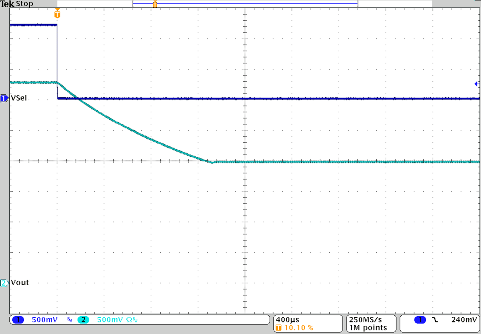 Figure 39. TPS62745 Output Voltage Change from 3.3 V to 2.0 V for IOUT = 10 mA