ZHCSE11A June 2015 – June 2015 TPS62745 , TPS627451
PRODUCTION DATA.
- 1 特性
- 2 应用
- 3 说明
- 4 典型应用电路原理图
- 5 修订历史记录
- 6 Device Comparison Table
- 7 Pin Configuration and Functions
- 8 Specifications
- 9 Detailed Description
- 10Application and Implementation
- 11Power Supply Recommendations
- 12Layout
- 13器件和文档支持
- 14机械、封装和可订购信息
8 Specifications
8.1 Absolute Maximum Ratings
Over operating free-air temperature range (unless otherwise noted) (1)| PIN | MIN | MAX | UNIT | |
|---|---|---|---|---|
| Voltage | VIN | –0.3 | 12 | V |
| SW, VIN_SW(2) | –0.3 | VIN +0.3 | V | |
| EN | –0.3 | VIN +0.3 | V | |
| EN_VIN_SW, VSEL1-4 | –0.3 | 6 | V | |
| PG | –0.3 | 6 | V | |
| VOUT | –0.3 | 3.6 | V | |
| Power Good Sink Current | PG | 10 | mA | |
| VIN Switch Output Current | VIN_SW | 10 | mA | |
| Junction temperature, TJ | –40 | 150 | °C | |
| Storage temperature, Tstg | –65 | 150 | °C | |
(1) Stresses beyond those listed under Absolute Maximum Ratings may cause permanent damage to the device. These are stress ratings only, which do not imply functional operation of the device at these or any other conditions beyond those indicated under Recommended Operating Conditions. Exposure to absolute-maximum-rated conditions for extended periods may affect device reliability.
(2) The DC voltage on the SW pin must not exceed 3.6 V
8.2 ESD Ratings
| VALUE | UNIT | |||
|---|---|---|---|---|
| V(ESD) | Electrostatic discharge | Human body model (HBM), per ANSI/ESDA/JEDEC JS-001, all pins(1) | ±2000 | V |
| Charged device model (CDM), per JEDEC specification JESD22-C101, all pins(2) | ±500 | |||
(1) JEDEC document JEP155 states that 500-V HBM allows safe manufacturing with a standard ESD control process.
(2) JEDEC document JEP157 states that 250-V CDM allows safe manufacturing with a standard ESD control process.
8.3 Recommended Operating Conditions
Over operating free-air temperature range (unless otherwise noted)| MIN | NOM | MAX | UNIT | ||
|---|---|---|---|---|---|
| Supply voltage VIN | 3.3 | 10 | V | ||
| Output current IOUT | VOUT + 0.7 V ≤ VIN ≤ 10 V | 300 | mA | ||
| Effective inductance | 2.8 | 4.7 | 6.2 | µH | |
| Capacitance connected to VIN pin | 3 | 10 | µF | ||
| Total effective capacitance connected to VOUT pin (1) | 5 | 10 | 22 | µF | |
| Operating junction temperature range, TJ | –40 | 125 | °C | ||
| Operating ambient temperature range, TA | –40 | 85 | °C | ||
(1) Due to the DC bias effect of ceramic capacitors, the effective capacitance is lower then the nominal value when a voltage is applied. This is why the capacitance is specified to allow the selection of the smallest capacitor required with the DC bias effect for this type of capacitor in mind. The nominal value given matches a typical capacitor to be chosen to meet the minimum capacitance required.
8.4 Thermal Information
| THERMAL METRIC(1) | TPS62745 | UNIT | |
|---|---|---|---|
| DSS | |||
| 12 PINS | |||
| RθJA | Junction-to-ambient thermal resistance | 61.8 | °C/W |
| RθJC(top) | Junction-to-case (top) thermal resistance | 70.9 | °C/W |
| RθJB | Junction-to-board thermal resistance | 25.7 | °C/W |
| ψJT | Junction-to-top characterization parameter | 1.9 | °C/W |
| ψJB | Junction-to-board characterization parameter | 25.7 | °C/W |
| RθJC(bot) | Junction-to-case (bottom) thermal resistance | 7.2 | °C/W |
(1) For more information about traditional and new thermal metrics, see the IC Package Thermal Metrics application report, SPRA953.
8.5 Electrical Characteristics
VIN = 6 V, TJ = –40°C to 125°C typical values are at TJ = 25°C (unless otherwise noted)| PARAMETER | TEST CONDITIONS | MIN | TYP | MAX | UNIT | ||
|---|---|---|---|---|---|---|---|
| SUPPLY | |||||||
| VIN | Input voltage range | VOUT + 0.7 V ≤ VIN ≤ 10 V ; min 3.3 V, whichever value is higher | 3.3 | 10 | V | ||
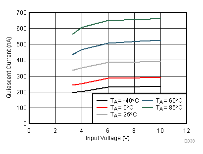
| IQ | Operating quiescent current | EN = VIN, device not switching; IOUT = 0 µA; VOUT = 2 V; TJ = –40°C to 85°C |
400 | 1960 | nA | ||
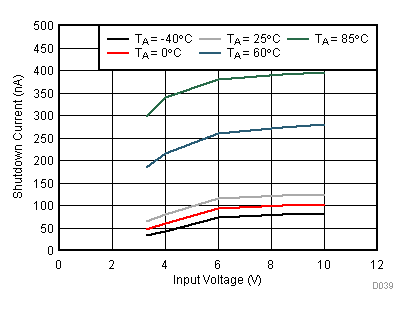
| ISD | Shutdown current | EN = GND, shutdown current into VIN; TJ = -40°C to 85°C |
130 | 1200 | nA | ||
| EN = GND, shutdown current into VIN; TJ = 60°C | 830 | ||||||
| VTH_UVLO+ | Undervoltage lockout threshold | Rising VIN; TJ = –40°C to 85°C | 3.1 | 3.3 | V | ||
| VTH_UVLO- | Falling VIN; TJ = –40°C to 85°C | 2.9 | 3.1 | ||||
| INPUTS (EN, EN_VIN_SW, VSEL1-4) | |||||||
| VIH TH | High level input voltage | VTH_UVLO- ≤ VIN ≤ 10 V | 1.2 | V | |||
| VIL TH | Low level input voltage | VTH_UVLO- ≤ VIN ≤ 10 V | 0.35 | V | |||
| IIN | Input bias current; except EN pin | TJ = 25°C | 10 | nA | |||
| TJ = 60°C | 20 | ||||||
| TJ = –40°C to 85°C | 50 | ||||||
| IIN | Input bias current for EN pin | TJ = 25°C | 20 | nA | |||
| TJ = 60°C | 40 | ||||||
| TJ = –40°C to 85°C | 100 | ||||||
| POWER SWITCHES | |||||||
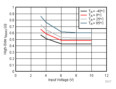
| RDS(ON) | High side MOSFET on-resistance | VIN = 4 V, I = 140 mA | 0.6 | 0.98 | Ω | ||
| Low side MOSFET on-resistance | 0.5 | 0.85 | |||||
| ILIMF | High side MOSFET DC switch current limit | 3.6 V ≤ VIN ≤ 10 V; device not in soft start | 480 | 600 | 720 | mA | |
| Low side MOSFET DC switch current limit | 600 | ||||||
| OUTPUT DISCHARGE SWITCH (VOUT) | |||||||
| RDSCH_VOUT | MOSFET on-resistance | EN = GND, IOUT = –10 mA into VOUT pin | 25 | 60 | Ω | ||
| IIN_VOUT | Bias current into VOUT pin(1) | EN = VIN, VOUT = 2 V | TJ = 25°C | 40 | 100 | nA | |
| TJ = –40°C to 85°C | 500 | ||||||
| INPUT VOLTAGE SWITCH (VIN_SW) | |||||||
| RDS(ON) | MOSFET on-resistance | EN_VIN_SW = High, IVIN_SW = 1 mA | 85 | 160 | Ω | ||
| IVIN_SW_LKG | VIN-switch leakage current | EN_VIN_SW = GND; leakage from VIN to VIN_SW when pulled to GND; TJ = –40°C to 85°C | -20 | 20 | nA | ||
| IVIN_SW | VIN-switch current | 5 | mA | ||||
| POWER GOOD OUTPUT (PG) | |||||||
| VTH_PG+ | Power good threshold voltage | Rising output voltage on VOUT pin | 95 | 97.5 | % | ||
| VTH_HYS | Power good threshold hysteresis | Falling output voltage on VOUT pin | 3 | ||||
| VOL | Low level output threshold | 3.3 V ≤ VIN ≤ 10 V, EN = GND, current into PG pin IPG = 4 mA |
0.3 | V | |||
| VOH | High level output threshold | 3.3 V ≤ VIN ≤ 10 V, EN = high, current into PG pin IPG = 0 mA |
6 | V | |||
| IIN_PG | Bias current into power good pin | PG pin is high impedance, VOUT = 2 V, EN = VIN, IOUT = 0 mA; TJ = –40°C to 85°C |
20 | nA | |||
| OUTPUT | |||||||
| ILIM_softstart | Switch current limit during soft start | Current limit is reduced during soft start, TJ = –40°C to 85°C |
40 | 110 | 180 | mA | |
| VVOUT | Output voltage range | For TPS627450; output voltages are selected with pins VSEL1 - 4 | 1.8 | 3.3 | V | ||
| For TPS627451; output voltages are selected with pins VSEL1 - 4 | 1.3 | 2.8 | |||||
| Output voltage accuracy | PFM mode, IOUT = 0 mA, VOUT + 0.6 V ≤ VIN ≤ 10 V; min 3.3 V, whichever value is higher; TJ = –40°C to 85°C |
-2.5 | 0 | 2.5 | % | ||
| PWM Mode, VOUT + 0.7 V ≤ VIN ≤ 10 V; min 3.3 V, whichever value is higher; TJ = –40°C to 85°C | –2 | 0 | 2 | ||||
| DC output voltage load regulation | VOUT = 2.0 V; IOUT = 2 mA to 80 mA (PFM mode) | 0.005 | %/mA | ||||
| DC output voltage load regulation | VOUT = 2.0 V; IOUT = 150 mA to 300 mA (PWM mode) | 0.001 | %/mA | ||||
| DC output voltage line regulation | VOUT = 2.0 V, IOUT = 300 mA, 4 V ≤ VIN ≤ 10 V | 0.015 | %/V | ||||
(1) A 50-MΩ (typical) internal resistor divider is internally connected to the VOUT pin
8.6 Timing Characteristics
VIN = 6 V, TJ = –40°C to 125°C typical values are at TJ = 25°C (unless otherwise noted)| PARAMETER | TEST CONDITIONS | MIN | TYP | MAX | UNIT | ||
|---|---|---|---|---|---|---|---|
| SUPPLY | |||||||
| tdelay | UVLO delay time | response time of UVLO circuit | 200 | µs | |||
| INPUT VOLTAGE SWITCH (VIN_SW) | |||||||
| tVIN_SW | VIN-switch turn-on settling time | Time from EN_VIN_SW = High until RDS(ON) is within specification | 100 | µs | |||
| POWER GOOD OUTPUT (PG) | |||||||
| tdelay | PGOOD delay time | Response time of PGOOD circuit; falling edge | 200 | µs | |||
| OUTPUT | |||||||
| tONmin | Minimum ON time | VIN = 6 V, VOUT = 2.0 V, IOUT = 0 mA | 256 | ns | |||
| tOFFmin | Minimum OFF time | VIN = 3.3 V | 50 | ns | |||
| tStart | Regulator start up time | VIN = 6 V, from transition EN = Low to High until device starts switching, TJ = -40°C to 85°C | 15 | 50 | ms | ||
| tSoftstart | Softstart time with reduced switch current limit | 3.3 V ≤ VIN ≤ 10 V, EN = VIN | 700 | µs | |||
8.7 Typical Characteristics

| EN = VIN, VOUT = 1.8 V, EN_VIN_SW = GND | Device Not Switching | |


| EN = GND, EN_VIN_SW = GND | ||
