ZHCSEV1A February 2016 – March 2016 TPS62770
PRODUCTION DATA.
- 1 特性
- 2 应用
- 3 说明
- 4 修订历史记录
- 5 Pin Configuration and Functions
- 6 Specifications
- 7 Detailed Description
-
8 Application and Implementation
- 8.1 Application Information
- 8.2
Typical Application
- 8.2.1 System and PMOLED Supply
- 8.2.2 Step-Up Converter with 5-V Output Voltage
- 8.2.3
Step-Up Converter Operating with Constant Output Current
- 8.2.3.1 Design Requirements
- 8.2.3.2
Detailed Design Procedure
- 8.2.3.2.1 Setting The Output Voltage Of The Step-Down Converter
- 8.2.3.2.2 Programming the Output Voltage Of The Step-Up Converter
- 8.2.3.2.3 Recommended LC Output Filter
- 8.2.3.2.4 Inductor Selection Step-Down Converter
- 8.2.3.2.5 Inductor Selection Step-Up Converter
- 8.2.3.2.6 DC/DC Input and Output Capacitor Selection
- 8.2.3.3 Application Curves
- 9 Power Supply Recommendations
- 10Layout
- 11器件和文档支持
- 12机械、封装和可订购信息
5 Pin Configuration and Functions
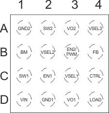
YFP Package
16-Pin DSBGA
Top View

Pin Functions
| PIN | I/O | DESCRIPTION | |
|---|---|---|---|
| NAME | NO | ||
| EN2/PWM | B3 | IN | Enable pin for the step-up converter. High level enables the devices, low level turns the device into shutdown mode. A PWM signal can be applied to this pin when used as a constant current driver (BM pin connected to VIN). The pin must be terminated. |
| GND2 | A1 | PWR | GND supply pin for the step-up converter. Connect this pin close to the GND terminals of the input and output capacitors. |
| SW2 | A2 | IN | The switch pin of the step-up converter. It is connected to the drain of the internal power MOSFET. Connect the inductor L2 between this pin and the input capacitor CIN |
| VO2 | A3 | OUT | Output of the step-up converter. |
| BM | B1 | IN | This pin controls the operation mode of the step-up converter. With BM = high, the device features a low feedback voltage of 200mV, which can be scaled down by the integrated PWM to analog converter. With BM = low, the device operates with a 0.8V feedback voltage and operates as a step-up converter with voltage regulation. This pin must be terminated and set before the device is enabled. |
| FB | B4 | IN | Feedback pin for the step-up converter to set the output voltage / current. Connect the pin to the center tap of a resistor divider to program the output voltage. When it is connected to the VIN pin, the output voltage is set to 12 V by an internal feedback divider network. When used as a LED current driver connect the sense resistor between this pin and GND. The LED string is connected between FB pin and VO2. |
| EN1 | C2 | IN | Enable pin for the step-down converter. High level enables the devices, low level turns the device into shutdown mode. The pin must be terminated. |
| VSEL1 | C3 | IN | Output voltage selection pins. See Output Voltage Setting Step-Down Converter for VOUT selection. These pins must be terminated. The pins can be dynamically changed during operation. |
| VSEL2 | B2 | IN | |
| VSEL3 | A4 | IN | |
| CTRL | C4 | IN | This pin controls the load switch between VO1 and LOAD. With CTRL = low, the LOAD switch is disabled. The pin must be terminated. |
| VIN | D1 | PWR | VIN power supply pin. Connect the input capacitor close to this pin for best noise and voltage spike suppression. A ceramic capacitor of 10μF is required. |
| GND1 | D2 | PWR | GND supply pin for the step-down converter. Connect this pin close to both, the GND terminal of the input and output capacitor. |
| SW1 | C1 | OUT | This is the switch pin of the step-down converter and is connected to the internal MOSFET switches. Connect the inductor L1 between this terminal and the output capacitor. |
| VO1 | D3 | OUT | Output of the step-down converter. The output voltage is sensed via this pin to the internal feedback divider network for the regulation loop. In addition the internal load switch is connected between VO1 pin and LOAD pin. Connect this pin directly to the output capacitor with a short trace. The pin is connected to GND1 and discharges the output capacitor when the converter is disabled. |
| LOAD | D4 | OUT | Output terminal of the internal load switch. With CTRL = high, the internal load switch connects VO1 to the LOAD pin. The switch features a slew rate control. This pin is pulled to GND with the CTRL = low. If not used, leave the pin open. |
5.1 Output Voltage Setting Step-Down Converter
| VO1 [V] | VSEL3 | VSEL2 | VSEL1 |
|---|---|---|---|
| 1.0 | 0 | 0 | 0 |
| 1.05 | 0 | 0 | 1 |
| 1.1 | 0 | 1 | 0 |
| 1.2 | 0 | 1 | 1 |
| 1.8 | 1 | 0 | 0 |
| 1.9 | 1 | 0 | 1 |
| 2.0 | 1 | 1 | 0 |
| 3.0 | 1 | 1 | 1 |