ZHCSJW0D June 2019 – March 2020 TPS62840
PRODUCTION DATA.
- 1 特性
- 2 应用
- 3 说明
- 4 修订历史记录
- 5 Device Comparison Table
- 6 Pin Configuration and Functions
- 7 Specifications
-
8 Detailed Description
- 8.1 Overview
- 8.2 Functional Block Diagram
- 8.3
Feature Description
- 8.3.1 Smart Enable and Shutdown
- 8.3.2 Soft Start
- 8.3.3 Mode Selection: Power-Save Mode (PFM/PWM) or Forced PWM Operation (FPWM)
- 8.3.4 Output Voltage Selection (VSET)
- 8.3.5 Undervoltage Lockout UVLO
- 8.3.6 Switch Current Limit / Short Circuit Protection
- 8.3.7 Output Voltage Discharge
- 8.3.8 Thermal Shutdown
- 8.3.9 STOP Mode
- 8.4 Device Functional Modes
- 9 Application and Implementation
- 10Power Supply Recommendations
- 11Layout
- 12器件和文档支持
- 13机械、封装和可订购信息
封装选项
机械数据 (封装 | 引脚)
散热焊盘机械数据 (封装 | 引脚)
- DLC|8
订购信息
6 Pin Configuration and Functions
DLC
SON-8

DGR
HVSSOP-8

YBG
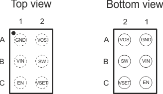
WCSP-6

Pin Functions
| PIN | I/O | DESCRIPTION | |||
|---|---|---|---|---|---|
| NAME | DLC
(SON-8) |
DGR
(HVSSOP-8) |
YBG
(WCSP-6) |
||
| VIN | 2 | 6 | B1 | PWR | VIN power supply pin. Connect the input capacitor close to this pin for best noise and voltage spike suppression. A 4.7-µF ceramic capacitor is required. |
| SW | 7 | 2 | B2 | PWR | The switch pin is connected to the internal MOSFET switches. Connect the inductor to this terminal. |
| GND | 1 | 8 | A1 | PWR | GND supply pin. Connect this pin close to the GND terminal of the input and output capacitors. |
| VSET | 5 | 4 | C2 | IN | Connecting a resistor to GND sets the output voltage when the converter is enabled. For the TPS62849, connect this pin to GND. |
| VOS | 8 | 1 | A2 | IN | Output voltage sense pin for the internal feedback divider network and regulation loop. When the converter is disabled, this pin discharges VOUT by an internal MOSFET. Connect this pin directly to the output capacitor with a short trace. |
| EN | 4 | 5 | C1 | IN | Enable pin. A high level enables the device and a low level turns the device off. The pin features an internal pulldown resistor, which is disabled once the device has started up and the output voltage is regulated. The pulldown resistor is activated again, once a low level has been detected. |
| STOP | 6 | n/a | n/a | IN | STOP Switching pin. When this pin is logic high, the converter stops switching in order to provide a quiet supply rail. The output is powered from the charge available in the output capacitor. When this pin is logic low, the device immediately resumes operation. The pin features an internal pulldown resistor, which is disabled once a high level is detected at the input. The pulldown resistor is activated again, once a low level has been detected. |
| MODE | 3 | 3 | n/a | IN | MODE pin. A low level enables Power-Save Mode operation with an automatic transition between PFM and PWM modes. A high level forces the converter to operated in PWM mode. This pin can be toggled during operation. It must be terminated. |
| NC | n/a | 7 | n/a | This pin is not connected internally. Do not connect this pin. | |
| EP | n/a | 9 | n/a | PWR | Exposed thermal pad(1). The PowerPAD must be connected to GND. |
(1) For more information about the PowerPAD, see the PowerPAD™ Thermally Enhanced Package application report.