ZHCSL99G September 2019 – January 2025 TPS62860 , TPS62861
PRODUCTION DATA
- 1
- 1 特性
- 2 应用
- 3 说明
- 4 Device Comparison Table
- 5 Pin Configuration and Functions
- 6 Specifications
- 7 Detailed Description
- 8 Register Map
- 9 Application and Implementation
- 10Device and Documentation Support
- 11Revision History
- 12Mechanical, Packaging, and Orderable Information
5 Pin Configuration and Functions
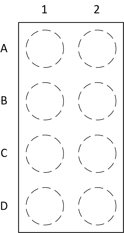
 Figure 5-1 8-Pin DSBGA YCH Package (Top
View)
Figure 5-1 8-Pin DSBGA YCH Package (Top
View)Table 5-1 Pin Functions, TPS628610, TPS628600, TPS628603,
TPS628604, TPS628605, and TPS628606
| PIN | TYPE | DESCRIPTION | |
|---|---|---|---|
| NAME | NO. | ||
| GND | D2 | PWR | GND supply pin. Connect this pin close to the GND terminal of the input and output capacitor. |
| VOS | D1 | IN | Output voltage sense pin for the internal feedback divider network and regulation loop. This pin also discharges VOUT by an internal MOSFET when the converter is disabled. Connect this pin directly to the output capacitor with a short trace. |
| VIN | C2 | PWR | VIN power supply pin. Connect the input capacitor close to this pin for best noise and voltage spike suppression. A ceramic capacitor is required. |
| SW | C1 | PWR | The switch pin is connected to the internal MOSFET switches. Connect the inductor to this terminal. |
| VSEL | B2 | IN | Voltage selection pin. Can be toggled during operation. LOW = 0.6 V (TPS628600, TPS628610), 1.05 V (TPS628603), HIGH = 1.1 V (TPS628600, TPS628610), 0.65 V (TPS628603) |
| EN | B1 | IN | A high level enables the devices and a low level turns the device off. The pin features an internal pulldown resistor, which is disabled after the device has started up. |
| SDA | A2 | IN | I2C serial data pin. Do not leave floating. |
| SCL | A1 | IN | I2C serial clock pin. Do not leave floating. |
Table 5-2 Pin Functions, TPS628601
| PIN | TYPE | DESCRIPTION | |
|---|---|---|---|
| NAME | NO. | ||
| GND | D2 | PWR | GND supply pin. Connect this pin close to the GND terminal of the input and output capacitor. |
| VOS | D1 | IN | Output voltage sense pin for the internal feedback divider network and regulation loop. This pin also discharges VOUT by an internal MOSFET when the converter is disabled. Connect this pin directly to the output capacitor with a short trace. |
| VIN | C2 | PWR | VIN power supply pin. Connect the input capacitor close to this pin for best noise and voltage spike suppression. A ceramic capacitor is required. |
| SW | C1 | PWR | The switch pin is connected to the internal MOSFET switches. Connect the inductor to this terminal. |
| PG | B2 | OUT | Open-drain power-good output |
| EN | B1 | IN | A high level enables the devices and a low level turns the device off. The pin features an internal pulldown resistor, which is disabled after the device has started up. |
| VSEL-1 | A2 | IN | Voltage Selection Pin. Can be toggled during operation. |
| VSEL-2 | A1 | IN | Voltage Selection Pin. Can be toggled during operation. |