ZHCSLJ2B September   2020  – July 2021 TPS62868 , TPS62869

PRODUCTION DATA  

  1. 特性
  2. 应用
  3. 说明
  4. Revision History
  5. Device Options
  6. Pin Configuration and Functions
  7. Specifications
    1. 7.1 Absolute Maximum Ratings
    2. 7.2 ESD Ratings
    3. 7.3 Recommended Operating Conditions
    4. 7.4 Thermal Information
    5. 7.5 Electrical Characteristics
    6. 7.6 I2C InterfaceTiming Characteristics
    7. 7.7 Typical Characteristics
  8. Detailed Description
    1. 8.1 Overview
    2. 8.2 Functional Block Diagram
    3. 8.3 Feature Description
      1. 8.3.1 Power Save Mode
      2. 8.3.2 Forced PWM Mode
      3. 8.3.3 100% Duty Cycle Mode Operation
      4. 8.3.4 Start-up
      5. 8.3.5 Switch Current Limit and HICCUP Short-Circuit Protection
      6. 8.3.6 Undervoltage Lockout (UVLO)
      7. 8.3.7 Thermal Warning and Shutdown
    4. 8.4 Device Functional Modes
      1. 8.4.1 Enable and Disable (EN)
      2. 8.4.2 Output Discharge
      3. 8.4.3 Start-Up Output Voltage and I2C Target Address Selection
        1. 8.4.3.1 TPS6286xxA Devices
        2. 8.4.3.2 TPS6286xxxC Devices
      4. 8.4.4 Select Output Voltage Registers (VID)
      5. 8.4.5 Power Good ( PG)
    5. 8.5 Programming
      1. 8.5.1 Serial Interface Description
      2. 8.5.2 Standard-, Fast-, and Fast-Mode Plus Protocol
      3. 8.5.3 HS-Mode Protocol
      4. 8.5.4 I2C Update Sequence
      5. 8.5.5 I2C Register Reset
    6. 8.6 Register Map
      1. 8.6.1 Target Address Byte
      2. 8.6.2 Register Address Byte
      3. 8.6.3 VOUT Register 1
      4. 8.6.4 VOUT Register 2
      5. 8.6.5 CONTROL Register
      6. 8.6.6 STATUS Register
  9. Application and Implementation
    1. 9.1 Application Information
    2. 9.2 Typical Application
      1. 9.2.1 Design Requirements
      2. 9.2.2 Detailed Design Procedure
        1. 9.2.2.1 Setting The Output Voltage
        2. 9.2.2.2 Output Filter Design
        3. 9.2.2.3 Inductor Selection
        4. 9.2.2.4 Capacitor Selection
      3. 9.2.3 Application Curves
    3. 9.3 Typical Application – TPS6286x0A and TPS6286x0xC Devices
      1. 9.3.1 Design Requirements
      2. 9.3.2 Detailed Design Procedure
        1. 9.3.2.1 Setting the Output Voltage
        2. 9.3.2.2 Output Filter Design
        3. 9.3.2.3 Inductor Selection
        4. 9.3.2.4 Capacitor Selection
      3. 9.3.3 Application Curves
  10. 10Power Supply Recommendations
  11. 11Layout
    1. 11.1 Layout Guidelines
    2. 11.2 Layout Example
      1. 11.2.1 Thermal Considerations
  12. 12Device and Documentation Support
    1. 12.1 Device Support
      1. 12.1.1 第三方米6体育平台手机版_好二三四免责声明
    2. 12.2 Documentation Support
      1. 12.2.1 Related Documentation
    3. 12.3 支持资源
    4. 12.4 接收文档更新通知
    5. 12.5 Trademarks
    6. 12.6 术语表
    7. 12.7 Electrostatic Discharge Caution
  13. 13Mechanical, Packaging, and Orderable Information

封装选项

机械数据 (封装 | 引脚)
散热焊盘机械数据 (封装 | 引脚)
订购信息

Pin Configuration and Functions

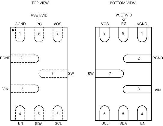
GUID-20200723-CA0I-S9RP-XK7Q-VHVPD8BJPXXF-low.gif Figure 6-1 9-Pin RQY QFN Package (Top View)
Table 6-1 Pin Functions
PIN DESCRIPTION
NAME NO.
AGND 1 Analog ground pin
VSET/VID 9 Start-up output voltage and device address selection pin. An external resistor must be connected.
After start-up, the pin can be used to select the VOUT registers for the output voltage (Low = VOUT register 1; high = VOUT register 2). See Section 8.4.4. This pin is pulled to GND when the device is in shutdown.
The function after start-up depends on the device option. See the Device Options.
PG 9 Power-good open-drain output pin. The pullup resistor can be connected to voltages up to 5.5 V. If unused, leave it floating. This pin is pulled to GND when the device is in shutdown.
The function after start-up depends on the device option. See Section 5.
VOS 8 Output voltage sense pin. This pin must be directly connected to the output capacitor.
PGND 2 Power ground pin
SW 7 Switch pin of the power stage
VIN 3 Power supply input voltage pin
EN 4 Device enable pin. To enable the device, this pin needs to be pulled high. Pulling this pin low disables the device. Do not leave floating.
SDA 5 I2C serial data pin. Do not leave it floating. Connect it to AGND if not used.
SCL 6 I2C serial clock pin. Do not leave it floating. Connect it to AGND if not used.