ZHCSM65 March 2022 TPS629203-Q1
PRODUCTION DATA
- 1 特性
- 2 应用
- 3 说明
- 4 Revision History
- 5 Device Comparison Table
- 6 Pin Configuration and Functions
- 7 Specifications
-
8 Detailed Description
- 8.1 Overview
- 8.2 Functional Block Diagram
- 8.3
Feature Description
- 8.3.1 Mode Selection and Device Configuration (MODE/S-CONF Pin)
- 8.3.2 Adjustable VO Operation (External Voltage Divider)
- 8.3.3 Selectable VO Operation (VSET and Internal Voltage Divider)
- 8.3.4 Smart Enable with Precise Threshold
- 8.3.5 Power Good (PG)
- 8.3.6 Output Discharge Function
- 8.3.7 Undervoltage Lockout (UVLO)
- 8.3.8 Current Limit and Short Circuit Protection
- 8.3.9 Thermal Shutdown
- 8.4 Device Functional Modes
- 9 Application and Implementation
- 10Power Supply Recommendations
- 11Layout
- 12Device and Documentation Support
- 13Mechanical, Packaging, and Orderable Information
6 Pin Configuration and Functions
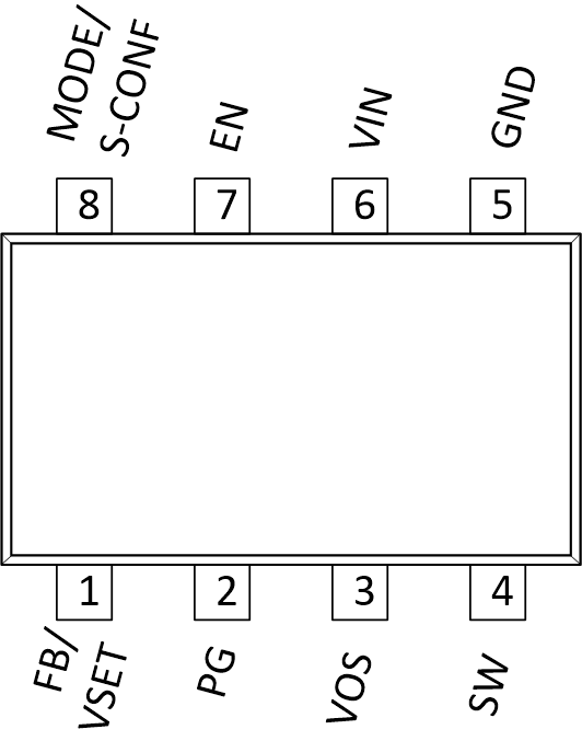
 Figure 6-1 TPS629203-Q1 8-Pin DRL SOT-5X3 Pinout
Table 6-1 Pin Functions
| Pin | I/O | Description | |
|---|---|---|---|
| Name | NO. | ||
| FB/VSET | 1 | I | Dependent upon device
configuration (see Section 8.3.1)
|
| PG | 2 | O | Open-drain power-good output |
| VOS | 3 | I | Output voltage sense pin. Connect directly to the positive pin of the output capacitor. |
| SW | 4 | Switch pin of the converter. Connected to the internal power switches | |
| GND | 5 | Ground pin | |
| VIN | 6 | I | Power supply input. Make sure the input capacitor is connected as close as possible between the VIN pin and GND. |
| EN | 7 | I | Enable/disable pin including a threshold comparator. Connect to logic low to disable the device. Pull high to enable the device. Do not leave this pin unconnected. |
| MODE/S-CONF | 8 | I | Device mode selection (auto PFM/PWM or forced PWM operation) and Smart-CONFIG pin. Connect a resistor to configure the device according to Table 8-1. |