ZHCSQD4A october   2022  – march 2023 TPS62993-Q1

PRODUCTION DATA  

  1. 特性
  2. 应用
  3. 说明
  4. Revision History
  5. Device Comparison Table
  6. Pin Configuration and Functions
  7. Specifications
    1. 7.1 Absolute Maximum Ratings
    2. 7.2 ESD Ratings
    3. 7.3 Recommended Operating Conditions
    4. 7.4 Thermal Information
    5. 7.5 Electrical Characteristics
    6. 7.6 Typical Characteristics
  8. Detailed Description
    1. 8.1 Overview
    2. 8.2 Functional Block Diagram
    3. 8.3 Feature Description
      1. 8.3.1  Mode Selection and Device Configuration MODE/S-CONF
      2. 8.3.2  Adjustable VO Operation (External Voltage Divider)
      3. 8.3.3  Selectable VO Operation (VSET and Internal Voltage Divider)
      4. 8.3.4  Soft Start and Tracking (SS/TR)
        1. 8.3.4.1 Tracking Function
      5. 8.3.5  Smart Enable with Precise Threshold
      6. 8.3.6  Power Good (PG)
      7. 8.3.7  Output Discharge Function
      8. 8.3.8  Undervoltage Lockout (UVLO)
      9. 8.3.9  Current Limit and Short-Circuit Protection
      10. 8.3.10 High Temperature Specifications
      11. 8.3.11 Thermal Shutdown
    4. 8.4 Device Functional Modes
      1. 8.4.1 Forced Pulse Width Modulation (FPWM) Operation
      2. 8.4.2 Power Save Mode Operation (Auto PFM and PWM)
      3. 8.4.3 AEE (Automatic Efficiency Enhancement)
      4. 8.4.4 100% Duty-Cycle Operation
      5. 8.4.5 Starting into a Prebiased Load
  9. Application and Implementation
    1. 9.1 Application Information
    2. 9.2 Typical Application with Adjustable Output Voltage
      1. 9.2.1 Design Requirements
      2. 9.2.2 Detailed Design Procedure
        1. 9.2.2.1 Custom Design With WEBENCH® Tools
        2. 9.2.2.2 Programming the Output Voltage
        3. 9.2.2.3 External Component Selection
          1. 9.2.2.3.1 Output Filter and Loop Stability
          2. 9.2.2.3.2 Inductor Selection
          3. 9.2.2.3.3 Capacitor Selection
            1. 9.2.2.3.3.1 Output Capacitor
            2. 9.2.2.3.3.2 Input Capacitor
            3. 9.2.2.3.3.3 Soft-Start Capacitor
      3. 9.2.3 Application Curves
        1. 9.2.3.1 Application Curves Vout = 1.8 V
        2. 9.2.3.2 Application Curves Vout = 1.2 V
        3. 9.2.3.3 Application Curves Vout = 0.6 V
    3. 9.3 Typical Application with Selectable VOUT using VSET
      1. 9.3.1 Design Requirements
      2. 9.3.2 Detailed Design Procedure
        1. 9.3.2.1 Programming the Output Voltage
      3. 9.3.3 Application Curves
        1. 9.3.3.1 Application Curves Vout = 5 V
        2. 9.3.3.2 Application Curves Vout = 3.3 V
    4. 9.4 System Examples
      1. 9.4.1 LED Power Supply
      2. 9.4.2 Powering Multiple Loads
      3. 9.4.3 Voltage Tracking
      4. 9.4.4 Inverting Buck-Boost (IBB)
    5. 9.5 Power Supply Recommendations
    6. 9.6 Layout
      1. 9.6.1 Layout Guidelines
      2. 9.6.2 Layout Example
      3. 9.6.3 Thermal Considerations
  10. 10Device and Documentation Support
    1. 10.1 Device Support
      1. 10.1.1 第三方米6体育平台手机版_好二三四免责声明
      2. 10.1.2 Development Support
        1. 10.1.2.1 Custom Design With WEBENCH® Tools
    2. 10.2 Documentation Support
      1. 10.2.1 Related Documentation
    3. 10.3 接收文档更新通知
    4. 10.4 支持资源
    5. 10.5 Trademarks
    6. 10.6 静电放电警告
    7. 10.7 术语表
  11. 11Mechanical, Packaging, and Orderable Information

封装选项

机械数据 (封装 | 引脚)
散热焊盘机械数据 (封装 | 引脚)
订购信息

Voltage Tracking

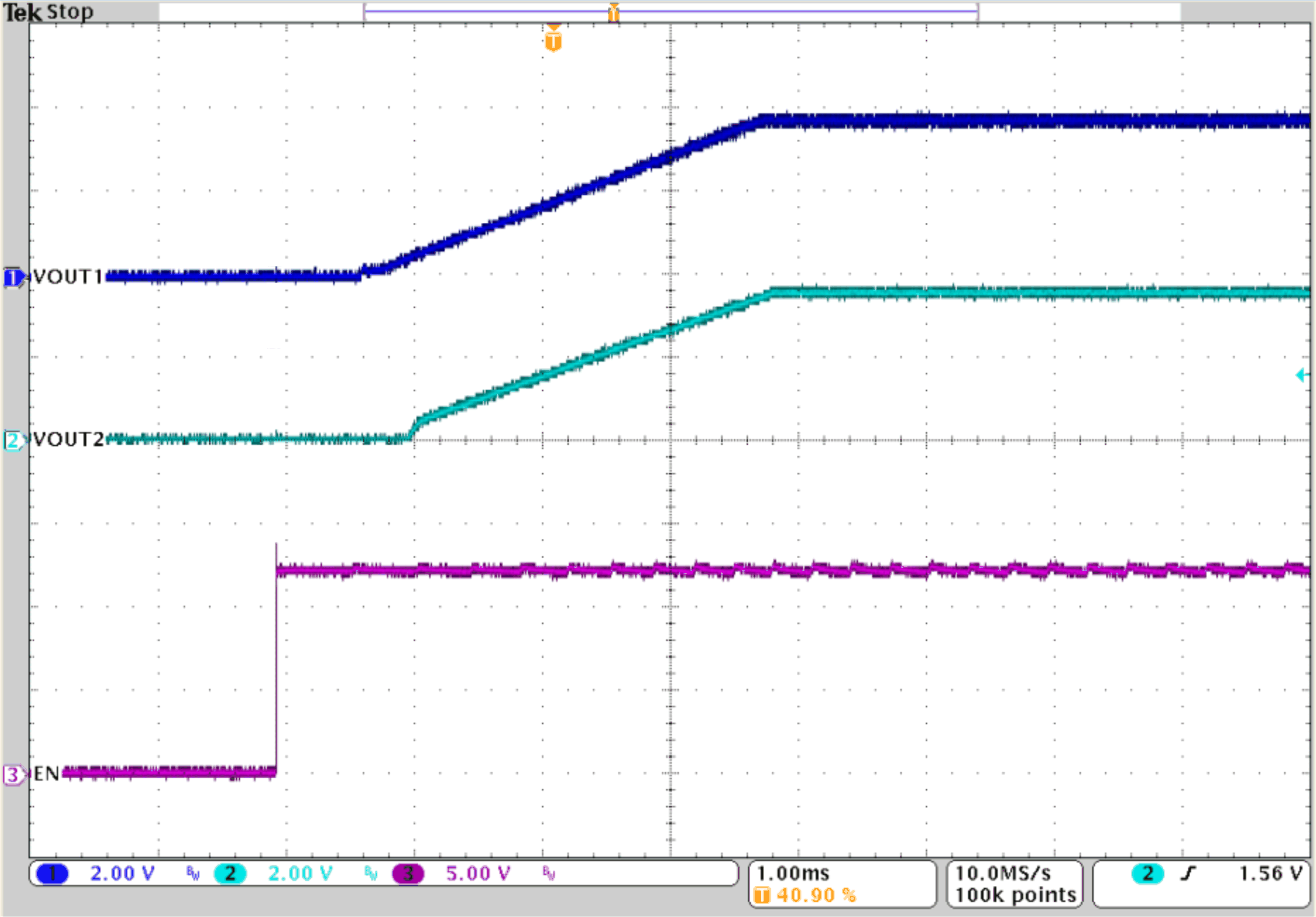
Figure 9-84 shows how two TPS62993-Q1s can be configured to tracking output voltages. In this configuration, Device 2 follows the voltage applied to its SS/TR pin from Device 1 output. A ramp on the SS/TR pin of Device 2 to 0.8 V in turn ramps VOUT2 according to the 0.6-V reference on VFB and the R4//R5 resistor divider.

For this example, to track the 3.8 V (VOUT1) of Device 1 a resistor divider (R7//R8) on SS/TR of Device 2 is required to generate 0.8 V when the output voltage (VOUT1) is in regulation. Due to the ISS current of 2.5 µA from the SS/TR pin, the equivalent resistance of R7 // R8 must be kept below 15 kΩ to minimize any offset the ISS current can cause on the SS/TR pin voltage.

GUID-20221004-SS0I-0ZN9-2B3B-NCWKLSJGD0TS-low.svg Figure 9-84 Tracking Example
GUID-99C4A0BD-1D11-4E98-803E-DAEBE44436B2-low.gif Figure 9-85 Tracking