SLVS520C March 2006 – October 2015 TPS63000 , TPS63001 , TPS63002
PRODUCTION DATA.
8 Application and Implementation
NOTE
Information in the following applications sections is not part of the TI component specification, and TI does not warrant its accuracy or completeness. TI’s customers are responsible for determining suitability of components for their purposes. Customers should validate and test their design implementation to confirm system functionality.
8.1 Application Information
The TPS6300x DC–DC converters are intended for systems powered by one-cell Li-ion or Li-polymer battery with a typical voltage between 2.3 V and 4.5 V. They can also be used in systems powered by a double or triple cell alkaline, NiCd, or NiMH battery with a typical terminal voltage between 1.8 V and 5.5 V. Additionally, any other voltage source with a typical output voltage between 1.8 V and 5.5 V can power systems where the TPS6300x is used.
8.2 Typical Application
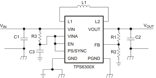 Figure 2. Typical Application Circuit for Adjustable Output Voltage Option
8.2.1 Design Requirements
The TPS63000 series of buck-boost converters have internal loop compensation. Therefore, the external LC filter has to be selected according to the internal compensation.
The design guideline provides a component selection to operate the device within the Recommended Operating Conditions.
For the fixed output voltage option the feedback pin needs to be connected to VOUT.
Table 1 shows the list of components for the application curves.
Table 1. List of Components
| REFERENCE | DESCRIPTION | MANUFACTURER |
|---|---|---|
| TPS63000 / TPS63001 / TPS63002 | Texas Instruments | |
| L1 | VLF4012-2R2 | TDK |
| C1 | 10 μF 6.3 V, 0603, X7R ceramic | |
| C2 | 2 × 10 μF 6.3 V, 0603, X7R ceramic | |
| C3 | 0.1 μF, X7R ceramic | |
| R3 | 100 Ω | |
| R1, R2 | Depending on the output voltage at TPS63000, not used at TPS63001 / TPS63002 | |
8.2.2 Detailed Design Procedure
8.2.2.1 Programming the Output Voltage
Within the TPS6300x family, there are fixed and adjustable output voltage versions available. To properly configure the fixed output voltage devices, the FB pin is used to sense the output voltage. This means that it must be connected directly to VOUT. At the adjustable output voltage versions, an external resistor divider is used to adjust the output voltage. The resistor divider must be connected between VOUT, FB and GND. When the output voltage is regulated properly, the typical value of the voltage at the FB pin is 500 mV. The maximum recommended value for the output voltage is 5.5 V. The current through the resistive divider should be about 100 times greater than the current into the FB pin. The typical current into the FB pin is 0.01 μA, and the voltage across the resistor between FB and GND, R2, is typically 500 mV. Based on those two values, the recommended value for R2 should be lower than 500 kΩ, in order to set the divider current at 1 μA or higher. TI recommends to keep the value for this resistor in the range of 200 kΩ. From that, the value of the resistor connected between VOUT and FB, R1, depending on the needed output voltage (VOUT), can be calculated using Equation 1.

If as an example, an output voltage of 3.3 V is needed, a 1-MΩ resistor should be chosen for R1. To improve control performance using a feedforward capacitor in parallel to R1 is recommended. The value for the feedforward capacitor can be calculated using Equation 2.

8.2.2.2 Inductor Selection
The inductor selection is affected by several parameter like inductor ripple current, output voltage ripple, transition point into power-save mode, and efficiency. See Table 2 for typical inductors.
Table 2. List of Recommended Inductors
| VENDOR | INDUCTOR SERIES |
|---|---|
| Coilcraft | LPS3015 |
| LPS4012 | |
| Murata | LQH3NP |
| Tajo Yuden | NR3015 |
| TDK | VLF3215 |
| VLF4012 |
For high efficiencies, the inductor should have a low DC resistance to minimize conduction losses. Especially at high-switching frequencies, the core material has a high impact on efficiency. When using small chip inductors, the efficiency is reduced mainly due to higher inductor core losses. This needs to be considered when selecting the appropriate inductor. The inductor value determines the inductor ripple current. The larger the inductor value, the smaller the inductor ripple current and the lower the conduction losses of the converter. Conversely, larger inductor values cause a slower load transient response. To avoid saturation of the inductor, the peak current for the inductor in steady-state operation is calculated using Equation 4. Only the equation which defines the switch current in boost mode is shown, because this provides the highest value of current and represents the critical current value for selecting the right inductor.


where
- D = Duty Cycle in Boost mode
- f = Converter switching frequency (typical 2.5MHz)
- L = Inductor value
- η = Estimated converter efficiency (use the number from the efficiency curves or 0.90 as an assumption)
NOTE
The calculation must be done for the minimum input voltage which is possible to have in boost mode.
Calculating the maximum inductor current using the actual operating conditions gives the minimum saturation current of the inductor needed. ITI recommends to choose an inductor with a saturation current 20% higher than the value calculated using Equation 4. Possible inductors are listed in Table 2.
8.2.2.3 Capacitor Selection
8.2.2.3.1 Input Capacitor
At least a 4.7-μF input capacitor is recommended to improve transient behavior of the regulator and EMI behavior of the total power supply circuit. A ceramic capacitor placed as close as possible to the VIN and PGND pins of the IC is recommended.
8.2.2.3.2 Output Capacitor
For the output capacitor, use of a small ceramic capacitors placed as close as possible to the VOUT and PGND pins of the IC is recommended. The recommended nominal output capacitance value is 15 µF.
There is also no upper limit for the output capacitance value. Larger capacitors causes lower output voltage ripple as well as lower output voltage drop during load transients.
8.2.3 Application Curves
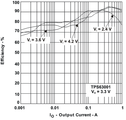
| VO = 3.3 V | Power Save enabled | |
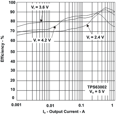
| VO = 5 V | Power Save enabled | |
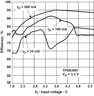
| VO = 3.3 V | Power Save enabled | |
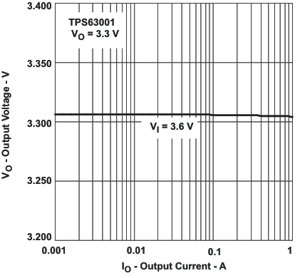
| VO = 3.3 V |
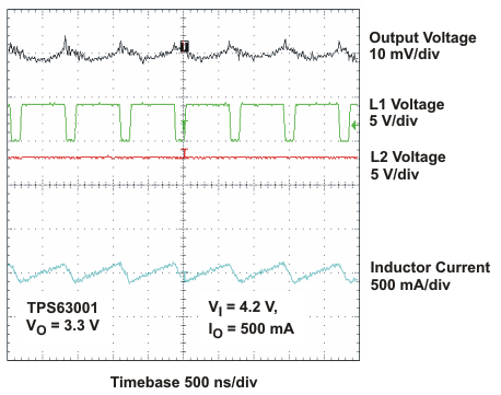
| VO = 3.3 V | VI = 4.2 V | IO = 500 mA |
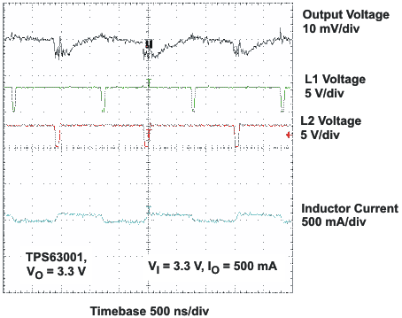
| VO = 3.3 V | VI = 3.3 V | IO = 500 mA |
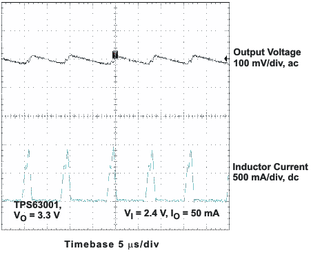
| VO = 3.3 V | VI = 2.4 V | IO = 50 mA |
(TPS63001, VIN < VOUT)
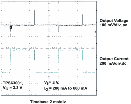
| VO = 3.3 V | VI = 3 V | IO = 200 mA to 600 mA |
(TPS63001, VIN < VOUT)
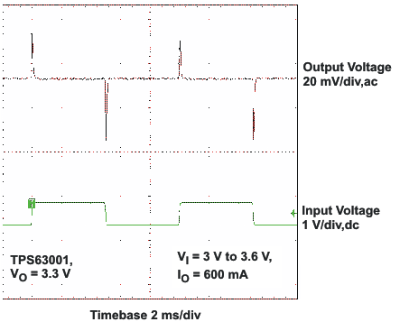
| VO = 3.3 V | VI = 3 V to 3.6 V | IO = 600 mA |
(TPS63001, IOUT= 600 mA)
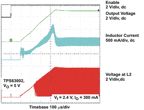
| VO = 5 V | VI = 2.4 V | IO = 300 mA |
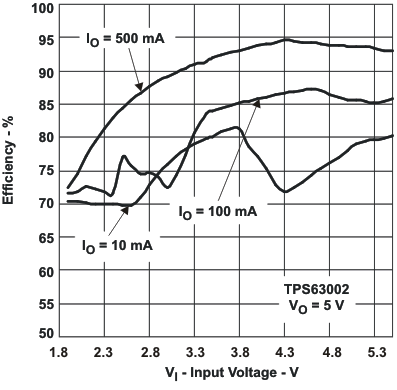
| VO = 5 V | Power Save enabled | |
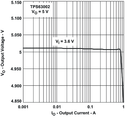
| VO = 5 V |
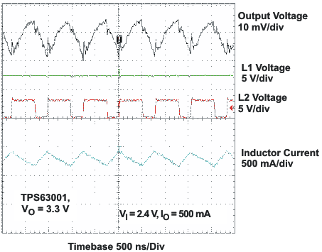
| VO = 3.3 V | VI = 2.4 V | IO = 500 mA |
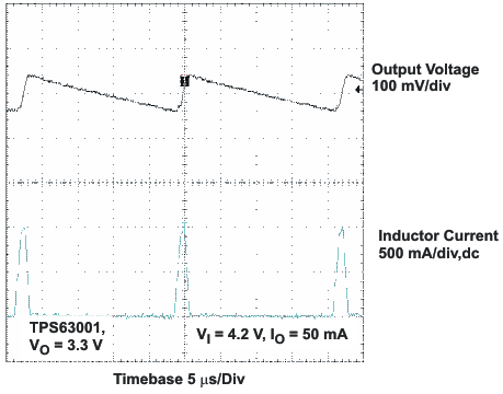
| VO = 3.3 V | VI = 4.2 V | IO = 50 mA |
(TPS63001, VIN > VOUT)
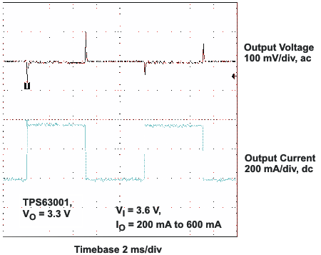
| VO = 3.3 V | VI = 3.6 V | IO = 200 mA to 600 mA |
(TPS63001, VIN > VOUT)
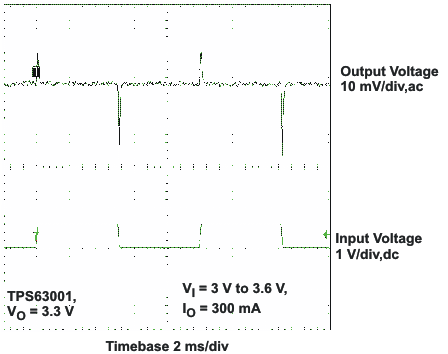
| VO = 3.3 V | VI = 3 V to 3.6 V | IO = 300 mA |
(TPS63001, IOUT = 300 mA)
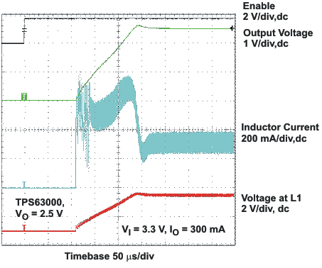
| VO = 2.5 V | VI = 3.3 V | IO = 300 mA |