SLVS653C June 2008 – February 2016 TPS63010 , TPS63011 , TPS63012
PRODUCTION DATA.
- 1 Features
- 2 Applications
- 3 Description
- 4 Revision History
- 5 Device Comparison Table
- 6 Pin Configuration and Functions
- 7 Specifications
- 8 Detailed Description
- 9 Application and Implementation
- 10Power Supply Recommendations
- 11Layout
- 12Device and Documentation Support
- 13Mechanical, Packaging, and Orderable Information
6 Pin Configuration and Functions
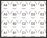
YFF Package
20-Pin DSBGA
Top View

Pin Functions
| PIN | I/O | DESCRIPTION | |
|---|---|---|---|
| NAME | NO. | ||
| EN | A4 | I | Enable input. (1 enabled, 0 disabled) |
| FB | E3 | I | Voltage feedback of adjustable versions, must be connected to VOUT at fixed output voltage versions |
| GND | C3, D3, E4 | — | Control and logic ground |
| L1 | B1,B2 | I | Connection for Inductor |
| L2 | D1,D2 | I | Connection for Inductor |
| PGND | C1,C2 | — | Power ground |
| PS | C4 | I | Enable and disable power save mode (1 disabled, 0 enabled) |
| SYNC | B4 | I | Clock signal for synchronization, should be connected to GND if not used |
| VIN | A1, A2 | I | Supply voltage for power stage |
| VINA | A3 | I | Supply voltage for control stage |
| VINA1 | B3 | O | Output of the 100 Ω for designing the VINA filter |
| VOUT | E1,E2 | O | Buck-boost converter output |
| VSEL | D4 | I | Output voltage select for fixed output voltage options (1 programs higher output voltage option, 0 programs lower output voltage option), must be connected to a defined logic signal at adjustable output voltage option. |