SLVS653C June 2008 – February 2016 TPS63010 , TPS63011 , TPS63012
PRODUCTION DATA.
- 1 Features
- 2 Applications
- 3 Description
- 4 Revision History
- 5 Device Comparison Table
- 6 Pin Configuration and Functions
- 7 Specifications
- 8 Detailed Description
- 9 Application and Implementation
- 10Power Supply Recommendations
- 11Layout
- 12Device and Documentation Support
- 13Mechanical, Packaging, and Orderable Information
8 Detailed Description
8.1 Overview
The TPS6301x uses 4 internal N-channel MOSFETs to maintain synchronous power conversion at all possible operating conditions. This enables the device to keep high efficiency over the complete input voltage and output power range. To regulate the output voltage at all possible input voltage conditions, the device automatically switches from buck operation to boost operation and back as required by the configuration. It always uses one active switch, one rectifying switch, one switch is held on, and one switch held off. Therefore, it operates as a buck converter when the input voltage is higher than the output voltage, and as a boost converter when the input voltage is lower than the output voltage. There is no mode of operation in which all 4 switches are switching at the same time. Keeping one switch on and one switch off eliminates their switching losses. The RMS current through the switches and the inductor is kept at a minimum, to minimize switching and conduction losses. Controlling the switches this way allows the converter to always keep higher efficiency. The device provides a seamless transition from buck-to-boost or from boost-to-buck operation
The device provides a seamless transition from buck-to-boost or from boost-to-buck operation.
8.2 Functional Block Diagrams
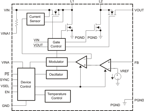
 Figure 22. Functional Block Diagram (TPS63010)
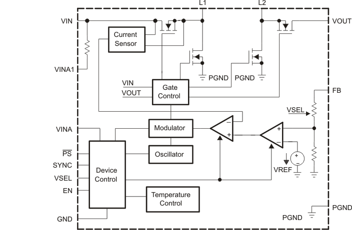
 Figure 23. Functional Block Diagram (TPS63011, TPS63012)
8.3 Feature Description
8.3.1 Output Voltage Selection
To program the output voltage at an adjustable device option, like the TPS63010, an external resistive feedback divider connected to FB must be used. For the fixed output voltage versions, FB is used as an output voltage sense and must be connected to the output voltage VOUT. All fixed output voltage versions have two different output voltages programmed internally. They are selected by programming high or low at VSEL. The higher output voltage is selected by programming VSEL high and the lower output voltage is selected by programming VSEL low. VSEL also supports standard logic thresholds.
8.3.2 Soft-Start and Short-Circuit Protection
After being enabled, the device starts operating. The average current limit ramps up from an initial 400 mA following the output voltage increasing. At an output voltage of about 1.2 V, the current limit is at its nominal value. If the output voltage does not increase, the current limit will not increase. There is no timer implemented. Thus, the output voltage overshoot at start-up, as well as the inrush current, is kept at a minimum. The device ramps up the output voltage in a controlled manner even if a very large capacitor is connected at the output. When the output voltage does not increase above 1.2 V, the device assumes a short-circuit at the output, and keeps the current limit low to protect itself and the application. At a short at the output during operation, the current limit is also decreased accordingly. At 0 V at the output, for example, the output current does not exceed about 400 mA.
8.3.3 Undervoltage Lockout
If the supply voltage on VINA is lower than its approximate threshold (see Electrical Characteristics), an undervoltage lockout function prevents device start-up. When in operation, the device automatically enters the shutdown mode if the voltage on VINA drops below the undervoltage lockout threshold. The device automatically restarts if the input voltage recovers to the minimum operating input voltage.
8.3.4 Overvoltage Protection
If, for any reason, the output voltage is not fed back properly to the input of the voltage amplifier, control of the output voltage will not work anymore. Therefore overvoltage protection is implemented to avoid the output voltage exceeding critical values for the device and possibly for the system it is supplying. The implemented overvoltage protection circuit monitors the output voltage internally as well. In case it reaches the overvoltage threshold the voltage amplifier regulates the output voltage to this value.
8.3.5 Overtemperature Protection
The device has a built-in temperature sensor which monitors the internal IC temperature. If the temperature exceeds the programmed threshold (see Electrical Characteristics), the device stops operating. As soon as the IC temperature has decreased below the programmed threshold, it again starts operating. There is a built-in hysteresis to avoid unstable operation at IC temperatures at the overtemperature threshold.
8.4 Device Functional Modes
8.4.1 Controller Circuit
The controlling circuit of the device is based on an average current mode topology. The average inductor current is regulated by a fast-current regulator loop which is controlled by a voltage control loop. The controller also uses input and output voltage feedforward. Changes of input and output voltage are monitored and immediately can change the duty cycle in the modulator to achieve a fast response to those errors. The voltage error amplifier gets its feedback input from the FB pin. At adjustable output voltages a resistive voltage divider must be connected to that pin. At fixed output voltages FB must be connected to the output voltage to directly sense the voltage. Fixed output voltage versions use a trimmed internal resistive divider. The feedback voltage will be compared with the internal reference voltage to generate a stable and accurate output voltage.
The controller circuit also senses the average input current as well as the peak input current. With this, maximum input power can be controlled as well as the maximum peak current to achieve a safe and stable operation under all possible conditions. To protect the device from overheating, an internal temperature sensor is implemented.
8.4.2 Synchronous Operation
The device uses 4 internal N-channel MOSFETs to maintain synchronous power conversion at all possible operating conditions. This enables the device to keep high efficiency over a wide input voltage and output power range.
To avoid ground shift problems due to the high currents in the switches, two separate ground pins GND and PGND are used. The reference for all control functions is the GND pin. The power switches are connected to PGND. Both grounds must be connected on the PCB at only one point ideally close to the GND pin. Due to the 4-switch topology, the load is always disconnected from the input during shutdown of the converter.
8.4.3 Buck-Boost Operation
To be able to regulate the output voltage properly at all possible input voltage conditions, the device automatically switches from step-down operation to boost operation and back as required by the configuration. It always uses one active switch, one rectifying switch, one switch permanently on, and one switch permanently off. Therefore, it operates as a step-down converter (buck) when the input voltage is higher than the output voltage, and as a boost converter when the input voltage is lower than the output voltage. There is no mode of operation in which all 4 switches are permanently switching. Controlling the switches this way allows the converter to maintain high efficiency at the most important point of operation; when input voltage is close to the output voltage. The RMS current through the switches and the inductor is kept at a minimum, to minimize switching and conduction losses. Switching losses are also kept low by using only one active and one passive switch. Regarding the remaining 2 switches, one is kept permanently on and the other is kept permanently off, thus causing no switching losses.
8.4.4 Power Save Mode
The PS pin can be used to select different operation modes. To enable power save, PS must be set low. Power save mode is used to improve efficiency at light load. If power save mode is enabled, the converter stops operating if the average inductor current gets lower than about 300 mA and the output voltage is at or above its nominal value. If the output voltage decreases below its nominal value, the device ramps up the output voltage again by starting operation using a programmed average inductor current higher than required by the current load condition. Operation can last for one or several pulses. The converter again stops operating once the conditions for stopping operation are met again.
The power save mode can be disabled by programming high at PS. The PS input supports standard logic threshold voltages. If the device is synchronized to an external clock connected to SYNC, power save mode is disabled.
8.4.5 Synchronization
Connecting a clock signal at SYNC forces the device to synchronize to the connected clock frequency. Synchronization is done by a PLL, so synchronizing to lower and higher frequencies compared to the internal clock works without any issues. The PLL can also tolerate missing clock pulses without the converter malfunctioning. The SYNC input supports standard logic thresholds. If synchronization is not used SYNC must be tied low or connected to GND. Applying a clock signal to SYNC automatically disables the power save mode.
8.4.6 Device Enable
The device is put into operation when EN is set high. It is put into a shutdown mode when EN is set to GND. In shutdown mode, the regulator stops switching, all internal control circuitry is switched off, and the load is disconnected from the input. This also means that the output voltage can drop below the input voltage during shutdown. During start-up of the converter, the duty cycle and the peak current are limited in order to avoid high peak currents flowing from the input.