ZHCSEB8 October 2015 TPS63020-Q1
PRODUCTION DATA.
- 1 特性
- 2 应用范围
- 3 说明
- 4 典型应用电路原理图
- 5 修订历史记录
- 6 Device Comparison Table
- 7 Pin Configuration and Functions
- 8 Specifications
- 9 Detailed Description
- 10Application and Implementation
- 11Power Supply Recommendations
- 12Layout
- 13器件和文档支持
- 14机械、封装和可订购信息
9 Detailed Description
9.1 Overview
The controller circuit of the device is based on an average current mode topology. The controller also uses input and output voltage feedforward. Changes of input and output voltage are monitored and immediately can change the duty cycle in the modulator to achieve a fast response to those errors. The voltage error amplifier gets its feedback input from the FB pin. At adjustable output voltages, a resistive voltage divider must be connected to that pin. At fixed output voltages, FB must be connected to the output voltage to directly sense the voltage. Fixed output voltage versions use a trimmed internal resistive divider. The feedback voltage will be compared with the internal reference voltage to generate a stable and accurate output voltage.
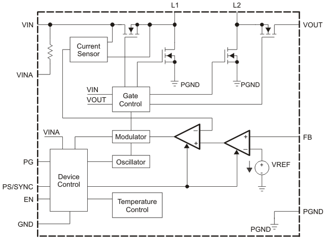
The device uses 4 internal N-channel MOSFETs to maintain synchronous power conversion at all possible operating conditions. This enables the device to keep high efficiency over a wide input voltage and output power range. To avoid ground shift problems due to the high currents in the switches, two separate ground pins GND and PGND are used. The reference for all control functions is the GND pin. The power switches are connected to PGND. Both grounds must be connected on the PCB at only one point, ideally, close to the GND pin. Due to the 4-switch topology, the load is always disconnected from the input during shutdown of the converter. To protect the device from overheating an internal temperature sensor is implemented.
9.2 Functional Block Diagram

9.3 Feature Description
9.3.1 Dynamic Voltage Positioning
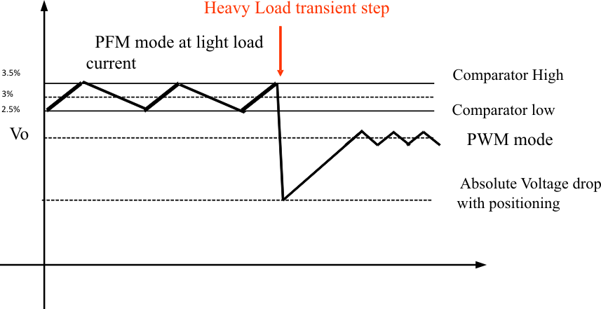
As detailed in Figure 3, the output voltage is typically 3% above the nominal output voltage at light load currents, as the device is in power save mode. This gives additional headroom for the voltage drop during a load transient from light load to full load. This allows the converter to operate with a small output capacitor and still have a low absolute voltage drop during heavy load transient changes. See Figure 3 for detailed operation of the power save mode.
9.3.2 Dynamic Current Limit
To protect the device and the application, the average inductor current is limited internally on the IC. At nominal operating conditions, this current limit is constant. The current limit value can be found in the electrical characteristics table. If the supply voltage at VIN drops below 2.3 V, the current limit is reduced. This can happen when the input power source becomes weak. Increasing output impedance, when the batteries are almost discharged, or an additional heavy pulse load is connected to the battery can cause the VIN voltage to drop. The dynamic current limit has its lowest value when reaching the minimum recommended supply voltage at VIN. At this voltage, the device is forced into burst mode operation trying to stay active as long as possible even with a weak input power source.
If the die temperature increases above the recommended maximum temperature, the dynamic current limit becomes active. Similar to the behavior when the input voltage at VIN drops, the current limit is reduced with temperature increasing.
9.3.2.1 Device Enable
The device is put into operation when EN is set high. It is put into a shutdown mode when EN is set to GND. In shutdown mode, the regulator stops switching, all internal control circuitry is switched off, and the load is disconnected from the input. This means that the output voltage can drop below the input voltage during shutdown. During start-up of the converter, the duty cycle and the peak current are limited in order to avoid high peak currents flowing from the input.
9.3.2.2 Power Good
The device has a built in power good function to indicate whether the output voltage is regulated properly. As soon as the average inductor current gets limited to a value below the current the voltage regulator demands for maintaining the output voltage the power good output gets low impedance. The output is open drain, so its logic function can be adjusted to any voltage level the connected logic is using, by connecting a pull up resistor to the supply voltage of the logic. By monitoring the status of the current control loop, the power good output provides the earliest indication possible for an output voltage break down and leaves the connected application a maximum time to safely react.
9.3.2.3 Overvoltage Protection
If, for any reason, the output voltage is not fed back properly to the input of the voltage amplifier, control of the output voltage will not work anymore. Therefore overvoltage protection is implemented to avoid the output voltage exceeding critical values for the device and possibly for the system it is supplying. The implemented overvoltage protection circuit monitors the output voltage internally as well. In case it reaches the overvoltage threshold the voltage amplifier regulates the output voltage to this value.
9.3.2.4 Undervoltage Lockout
An undervoltage lockout function prevents device start-up if the supply voltage at VINA is lower than approximately its threshold (see electrical characteristics table). When in operation, the device automatically enters the shutdown mode if the voltage at VINA drops below the undervoltage lockout threshold. The device automatically restarts if the input voltage recovers to the minimum operating input voltage.
9.3.2.5 Overtemperature Protection
The device has a built-in temperature sensor which monitors the internal IC temperature. If the temperature exceeds the programmed threshold (see electrical characteristics table) the device stops operating. As soon as the IC temperature has decreased below the programmed threshold, it starts operating again. There is a built-in hysteresis to avoid unstable operation at IC temperatures at the overtemperature threshold.
9.4 Device Functional Modes
9.4.1 Softstart and Short Circuit Protection
After being enabled, the device starts operating. The average current limit ramps up from an initial 400 mA following the output voltage increasing. At an output voltage of about 1.2 V, the current limit is at its nominal value. If the output voltage does not increase, the current limit will not increase. There is no timer implemented. Thus, the output voltage overshoot at startup, as well as the inrush current, is kept at a minimum. The device ramps up the output voltage in a controlled manner even if a large capacitor is connected at the output. When the output voltage does not increase above 1.2 V, the device assumes a short circuit at the output, and keeps the current limit low to protect itself and the application. At a short on the output during operation, the current limit also is decreased accordingly.
9.4.2 Buck-Boost Operation
To regulate the output voltage at all possible input voltage conditions, the device automatically switches from step down operation to boost operation and back as required by the configuration. It always uses one active switch, one rectifying switch, one switch permanently on, and one switch permanently off. Therefore, it operates as a step down converter (buck) when the input voltage is higher than the output voltage, and as a boost converter when the input voltage is lower than the output voltage. There is no mode of operation in which all 4 switches are permanently switching. Controlling the switches this way allows the converter to maintain high efficiency at the most important point of operation, when input voltage is close to the output voltage. The RMS current through the switches and the inductor is kept at a minimum, to minimize switching and conduction losses. For the remaining 2 switches, one is kept permanently on and the other is kept permanently off, thus causing no switching losses.
9.4.3 Control Loop
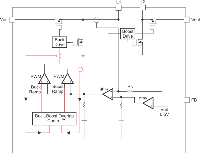
The controller circuit of the device is based on an average current mode topology. The average inductor current is regulated by a fast current regulator loop which is controlled by a voltage control loop. Figure 2 shows the control loop.
The non inverting input of the transconductance amplifier, gmv, is assumed to be constant. The output of gmv defines the average inductor current. The inductor current is reconstructed by measuring the current through the high side buck MOSFET. This current corresponds exactly to the inductor current in boost mode. In buck mode the current is measured during the on time of the same MOSFET. During the off time, the current is reconstructed internally starting from the peak value at the end of the on time cycle. The average current and the feedback from the error amplifier gmv forms the correction signal gmc. This correction signal is compared to the buck and the boost sawtooth ramp giving the PWM signal. Depending on which of the two ramps the gmc output crosses either the Buck or the Boost stage is initiated. When the input voltage is close to the output voltage, one buck cycle is always followed by a boost cycle. In this condition, no more than three cycles in a row of the same mode are allowed. This control method in the buck-boost region ensures a robust control and the highest efficiency.
The Buck-Boost Overlap ControlTM makes sure that the classical buck-boost function, which would cause two switches to be on every half a cycle, is avoided. Thanks to this block whenever all switches becomes active during one clock cycle, the two ramps are shifted away from each other, on the other hand when there is no switching activities because there is a gap between the ramps, the ramps are moved closer together. As a result the number of classical buck-boost cycles or no switching is reduced to a minimum and high efficiency values has been achieved.
 Figure 2. Average Current Mode Control
9.4.4 Power Save Mode and Synchronization
The PS/SYNC pin can be used to select different operation modes. Power save mode is used to improve efficiency at light load. To enable power-save, PS/SYNC must be set low. If PS/SYNC is set low then power save mode is entered when the average inductor current gets lower then about 100 mA. At this point the converter operates with reduced switching frequency and with a minimum quiescent current to maintain high efficiency.
During the power save mode, the output voltage is monitored with a comparator by the threshold comp low and comp high. When the device enters power save mode, the converter stops operating and the output voltage drops. The slope of the output voltage depends on the load and the value of output capacitance. As the output voltage falls below the comp low threshold set to 2.5% typical above VOUT, the device ramps up the output voltage again, by starting operation using a programmed average inductor current higher than required by the current load condition. Operation can last one or several pulses. The converter continues these pulses until the comp high threshold, set to typically 3.5% above VOUT nominal, is reached and the average inductance current gets lower than about 100 mA. When the load increases above the minimum forced inductor current of about 100 mA, the device will automatically switch to PWM mode.
The power save mode can be disabled by programming high at the PS/SYNC. Connecting a clock signal at PS/SYNC forces the device to synchronize to the connected clock frequency.
Synchronization is done by a PLL, so synchronizing to lower and higher frequencies compared to the internal clock works without any issues. The PLL can also tolerate missing clock pulses without the converter malfunctioning. The PS/SYNC input supports standard logic thresholds.
 Figure 3. Power Save Mode Thresholds and Dynamic Voltage Positioning