ZHCSJG8I July   2010  – October 2019 TPS63020 , TPS63021

PRODUCTION DATA.  

  1. 特性
  2. 应用
  3. 说明
    1.     Device Images
      1.      简化电路原理图
      2.      效率与输出电流间的关系
  4. 修订历史记录
  5. Pin Configuration and Functions
    1.     Pin Functions
  6. Specifications
    1. 6.1 Absolute Maximum Ratings
    2. 6.2 ESD Ratings
    3. 6.3 Recommended Operating Conditions
    4. 6.4 Thermal Information
    5. 6.5 Electrical Characteristics
    6. 6.6 Typical Characteristics
  7. Detailed Description
    1. 7.1 Overview
    2. 7.2 Functional Block Diagram
    3. 7.3 Feature Description
      1. 7.3.1 Dynamic Voltage Positioning
      2. 7.3.2 Dynamic Current Limit
      3. 7.3.3 Device Enable
      4. 7.3.4 Power Good
      5. 7.3.5 Overvoltage Protection
      6. 7.3.6 Undervoltage Lockout
      7. 7.3.7 Overtemperature Protection
    4. 7.4 Device Functional Modes
      1. 7.4.1 Soft-start and Short Circuit Protection
      2. 7.4.2 Buck-Boost Operation
      3. 7.4.3 Control Loop
      4. 7.4.4 Power Save Mode and Synchronization
  8. Application and Implementation
    1. 8.1 Application Information
    2. 8.2 Typical Application
      1. 8.2.1 Design Requirements
      2. 8.2.2 Detailed Design Procedure
        1. 8.2.2.1 Custom Design with WEBENCH Tools
        2. 8.2.2.2 Inductor Selection
        3. 8.2.2.3 Output Capacitor Selection
        4. 8.2.2.4 Input Capacitor Selection
        5. 8.2.2.5 Bypass Capacitor
      3. 8.2.3 Setting The Output Voltage
      4. 8.2.4 Application Curves
    3. 8.3 System Examples
      1. 8.3.1 Improved Transient Response for 2 A Load Current
      2. 8.3.2 Supercapacitor Backup Power Supply With Active Cell Balancing
      3. 8.3.3 Low-Power TEC Driver
  9. Power Supply Recommendations
  10. 10Layout
    1. 10.1 Layout Guidelines
    2. 10.2 Layout Example
    3. 10.3 Thermal Considerations
  11. 11器件和文档支持
    1. 11.1 接收文档更新通知
    2. 11.2 器件支持
      1. 11.2.1 使用 WEBENCH 工具创建定制设计方案
      2. 11.2.2 第三方米6体育平台手机版_好二三四免责声明
    3. 11.3 文档支持
      1. 11.3.1 相关文档
    4. 11.4 相关链接
    5. 11.5 支持资源
    6. 11.6 商标
    7. 11.7 静电放电警告
    8. 11.8 Glossary
  12. 12机械、封装和可订购信息

封装选项

机械数据 (封装 | 引脚)
散热焊盘机械数据 (封装 | 引脚)
订购信息

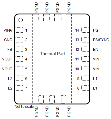
Pin Configuration and Functions

DSJ Package
14-Pin VSON with Exposed Thermal Pad
Top View
TPS63020 TPS63021 DSJ_son_pin_diagram.gif

Pin Functions

PIN I/O DESCRIPTION
NAME NO.
EN 12 I Enable input (1 enabled, 0 disabled), must not be left open
FB 3 I Voltage feedback of adjustable versions, must be connected to VOUT on fixed output voltage versions
GND 2 Control / logic ground
L1 8, 9 I Connection for inductor
L2 6, 7 I Connection for inductor
PG 14 O Output power good (1 good, 0 failure; open-drain), can be left open
PGND Power ground
PS/SYNC 13 I Enable / disable power save mode (1 disabled, 0 enabled, clock signal for synchronization), must not be left open
VIN 10, 11 I Supply voltage for power stage
VINA 1 I Supply voltage for control stage
VOUT 4, 5 O Buck-boost converter output
Exposed Thermal Pad The exposed thermal pad is connected to PGND.