8.2.1 Design Requirements
The design guideline provides a component selection to operate the device within the recommended operating conditions.
Table 1 shows the list of components for the Application Characteristic Curves.
Table 1. Components for Application Characteristic Curves(1)
| REFERENCE |
DESCRIPTION |
MANUFACTURER |
|
TPS63024 |
Texas Instruments |
| L1 |
1 μH, 8.75A, 13mΩ, SMD |
XAL4020-102MEB, Coilcraft |
| C1 |
10 μF 6.3V, 0603, X5R ceramic |
Standard |
| C2,C3 |
22 μF 6.3V, 0603, X5R ceramic |
Standard |
| R1 |
560kΩ |
Standard |
| R2 |
180kΩ |
Standard |
8.2.2 Detailed Design Procedure
The first step is the selection of the output filter components. To simplify this process Table 2 outline possible inductor and capacitor value combinations.
8.2.2.1 Output Filter Design
Table 2. Matrix of Output Capacitor and Inductor Combinations
NOMINAL INDUCTOR
VALUE [µH](1) |
NOMINAL OUTPUT CAPACITOR VALUE [µF](2) |
| 44 |
47 |
66 |
88 |
100 |
| 0.680 |
|
|
+ |
+ |
+ |
| 1.0 |
+(3) |
+ |
+ |
+ |
+ |
| 1.5 |
|
|
+ |
+ |
+ |
(1) Inductor tolerance and current de-rating is anticipated. The effective inductance can vary by 20% and –30%.
(2) Capacitance tolerance and bias voltage de-rating is anticipated. The effective capacitance can vary by 20% and –50%.
(3) Typical application. Other check mark indicates recommended filter combinations
8.2.2.2 Inductor Selection
The inductor selection is affected by several parameter like inductor ripple current, output voltage ripple, transition point into Power Save Mode, and efficiency. See Table 3 for typical inductors.
Table 3. List of Recommended Inductors(1)
| INDUCTOR VALUE |
COMPONENT SUPPLIER |
SIZE (LxWxH mm) |
Isat/DCR |
| 1 µH |
Coilcraft XAL4020-102ME |
4 X 4 X 2.10 |
4.5A/10mΩ |
| 1 µH |
Toko, DFE322512C |
3.2 X 2.5 X 1.2 |
4.7A/34mΩ |
| 1 µH |
TDK, SPM4012 |
4.4 X 4.1 X 1.2 |
4.1A/38mΩ |
| 1 µH |
Wuerth, 74438334010 |
3 X 3 X 1.2 |
6.6A/42.10mΩ |
| 0.6 µH |
Coilcraft XFL4012-601ME |
4 X 4 X 1.2 |
5A/17.40mΩ |
| 0.68µH |
Wuerth,744383340068 |
3 X 3 X 1.2 |
7.7A/36mΩ |
For high efficiencies, the inductor should have a low dc resistance to minimize conduction losses. Especially at high-switching frequencies, the core material has a high impact on efficiency. When using small chip inductors, the efficiency is reduced mainly due to higher inductor core losses. This needs to be considered when selecting the appropriate inductor. The inductor value determines the inductor ripple current. The larger the inductor value, the smaller the inductor ripple current and the lower the conduction losses of the converter. Conversely, larger inductor values cause a slower load transient response. To avoid saturation of the inductor, the peak current for the inductor in steady state operation is calculated using Equation 6. Only the equation which defines the switch current in boost mode is shown, because this provides the highest value of current and represents the critical current value for selecting the right inductor.
Equation 5. 
Equation 6. 
where
- D =Duty Cycle in Boost mod
- ƒ = Converter switching frequency (typical 2.5MHz)
- L = Inductor value
- η = Estimated converter efficiency (use the number from the efficiency curves or 0.90 as an assumption)
-
Note: The calculation must be done for the minimum input voltage which is possible to have in boost mode
Calculating the maximum inductor current using the actual operating conditions gives the minimum saturation current of the inductor needed. It's recommended to choose an inductor with a saturation current 20% higher than the value calculated using Equation 6. Possible inductors are listed in Table 3.
8.2.2.3 Capacitor Selection
8.2.2.3.1 Input Capacitor
At least a 10μF input capacitor is recommended to improve line transient behavior of the regulator and EMI behavior of the total power supply circuit. An X5R or X7R ceramic capacitor placed as close as possible to the VIN and PGND pins of the IC is recommended. This capacitance can be increased without limit. If the input supply is located more than a few inches from the TPS63024x converter additional bulk capacitance may be required in addition to the ceramic bypass capacitors. An electrolytic or tantalum capacitor with a value of 47 μF is a typical choice.
8.2.2.3.2 Output Capacitor
For the output capacitor, use of a small ceramic capacitors placed as close as possible to the VOUT and PGND pins of the IC is recommended. The recommended nominal output capacitance value is 20 µF with a variance as outlined in Table 2.
There is also no upper limit for the output capacitance value. Larger capacitors causes lower output voltage ripple as well as lower output voltage drop during load transients.
8.2.2.4 Setting The Output Voltage
When the adjustable output voltage version TPS63024x is used, the output voltage is set by an external resistor divider. The resistor divider must be connected between VOUT, FB and GND. When the output voltage is regulated properly, the typical value of the voltage at the FB pin is 800mV. The current through the resistive divider should be about 10 times greater than the current into the FB pin. The typical current into the FB pin is 0.1μA, and the voltage across the resistor between FB and GND, R2, is typically 800 mV. Based on these two values, the recommended value for R2 should be lower than 180kΩ, in order to set the divider current at 4μA or higher. It is recommended to keep the value for this resistor in the range of 180kΩ. From that, the value of the resistor connected between VOUT and FB, R1, depending on the needed output voltage (VOUT), can be calculated using Equation 7:
Equation 7. 
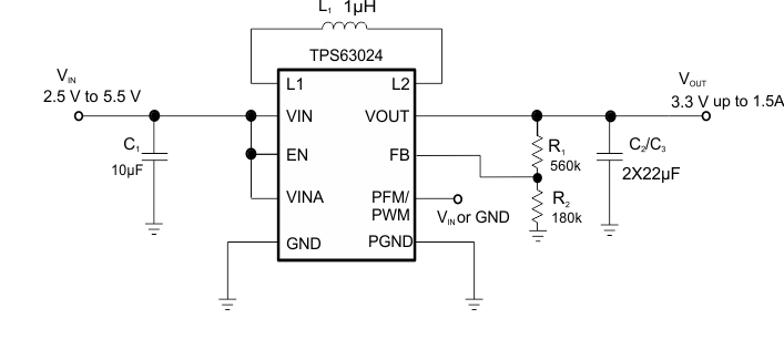 Figure 7. 3.3-V Adjustable Version


