ZHCSDM2A November   2014  – December 2014 TPS63024 , TPS630241 , TPS630242

PRODUCTION DATA.  

  1. 特性
  2. 应用范围
  3. 说明
  4. 修订历史记录
  5. Pin Configuration and Functions
  6. Specifications
    1. 6.1 Absolute Maximum Ratings
    2. 6.2 ESD Ratings
    3. 6.3 Recommended Operating Conditions
    4. 6.4 Thermal Information
    5. 6.5 Electrical Characteristics
    6. 6.6 Timing Requirements
    7. 6.7 Typical Characteristics
  7. Detailed Description
    1. 7.1 Overview
    2. 7.2 Functional Block Diagram
    3. 7.3 Feature Description
      1. 7.3.1 Undervoltage Lockout (UVLO)
      2. 7.3.2 Output Discharge Function
      3. 7.3.3 Thermal Shutdown
      4. 7.3.4 Softstart
      5. 7.3.5 Short Circuit Protection
    4. 7.4 Device Functional Modes
      1. 7.4.1 Control Loop Description
      2. 7.4.2 Power Save Mode Operation
      3. 7.4.3 Current Limit
      4. 7.4.4 Supply and Ground
      5. 7.4.5 Device Enable
  8. Application and Implementation
    1. 8.1 Application Information
    2. 8.2 Typical Application
      1. 8.2.1 Design Requirements
      2. 8.2.2 Detailed Design Procedure
        1. 8.2.2.1 Output Filter Design
        2. 8.2.2.2 Inductor Selection
        3. 8.2.2.3 Capacitor Selection
          1. 8.2.2.3.1 Input Capacitor
          2. 8.2.2.3.2 Output Capacitor
        4. 8.2.2.4 Setting The Output Voltage
      3. 8.2.3 Application Curves
  9. Power Supply Recommendations
  10. 10Layout
    1. 10.1 Layout Guidelines
    2. 10.2 Layout Example
  11. 11器件和文档支持
    1. 11.1 器件支持
      1. 11.1.1 Third-Party Products Disclaimer
    2. 11.2 文档支持
      1. 11.2.1 相关文档 
    3. 11.3 相关链接
    4. 11.4 商标
    5. 11.5 静电放电警告
    6. 11.6 Glossary
  12. 12机械、封装和可订购信息

封装选项

机械数据 (封装 | 引脚)
散热焊盘机械数据 (封装 | 引脚)
订购信息

Layout

Layout Guidelines

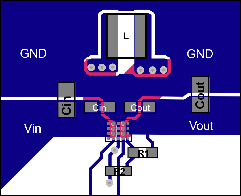
The PCB layout is an important step to maintain the high performance of the TPS63024x devices.

  • Place input and output capacitors as close as possible to the IC. Traces need to be kept short. Routing wide and direct traces to the input and output capacitor results in low trace resistance and low parasitic inductance.
  • Use a common-power GND.
  • The sense trace connected to FB is signal trace. Keep these traces away from L1 and L2 nodes.

Layout Example

TPS63024 TPS630241 TPS630242 PWR553_Layout_suggestion.gif Figure 30. TPS63024x Layout